Datasheet Details
Part number:
CDC2516
Manufacturer:
File Size:
1.07 MB
Description:
3.3-v phase-lock-loop clock driver.
Datasheet Details
Part number:
CDC2516
Manufacturer:
File Size:
1.07 MB
Description:
3.3-v phase-lock-loop clock driver.
CDC2516, 3.3-V Phase-Lock-Loop Clock Driver
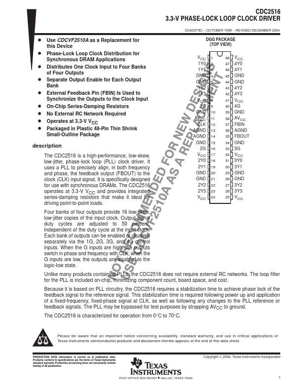
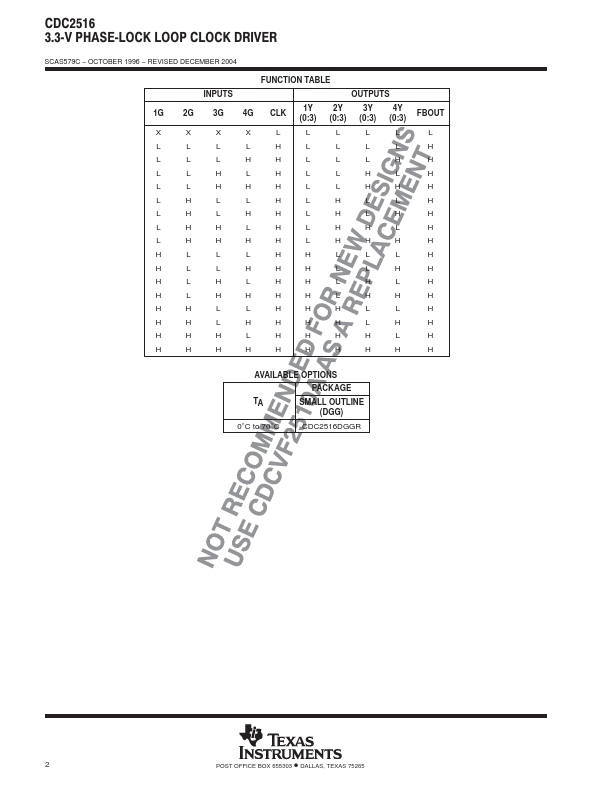
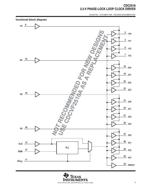
The CDC2516 is a high-performance, low-skew, low-jitter, phase-lock loop (PLL) clock driver.
It uses a PLL to precisely align, in both frequency and phase, the feedback output (FBOUT) to the clock (CLK) input signal.
It is specifically designed for use with synchronous DRAMs.
The CDC2516 operates at
CDC2516 3.3ĆV PHASEĆLOCK LOOP CLOCK DRIVER ą SCAS579C OCTOBER 1996 REVISED DECEMBER 2004 D Use CDCVF2510A as a Replacement for this Device D Phase-Lock Loop Clock Distribution for Synchronous DRAM Applications D Distributes One Clock Input to Four Banks of Four Outputs D Separate Output Enable for Each Output Bank D External Feedback Pin (FBIN) Is Used to Synchronize the Outputs to the Clock Input D On-Chip Series-Damping Resistors D No External RC Network Required D Operate
📁 Related Datasheet
📌 All Tags