Description
Input Clock Input Clock for Output Data Output Echo Clock DLL Disable when low Address Inputs Data Inputs 1 NOTE
Q0-35
Data Outputs Read, Write Control Pin, Read active when high Synchronous Load Pin, bus Cycle sequence is to be defined when low Block Write Control Pin,active when low Input Reference Voltage Output Driver Impedance Control Input Power Supply ( 1.8 V ) Output Power Supply ( 1.5V or 1.8V ) Ground JTAG Test Mode Select JTAG Test Data Input JTAG Test Clock JTAG Test Data Output No
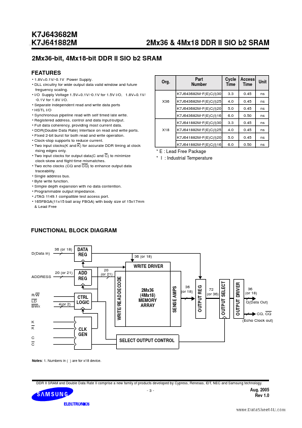
Features
- 1.8V+0.1V/-0.1V Power Supply.
- DLL circuitry for wide output data valid window and future freguency scaling.
- I/O Supply Voltage 1.5V+0.1V/-0.1V for 1.5V I/O, 1.8V+0.1V/ -0.1V for 1.8V I/O.
- Separate independent read and write data ports.
- HSTL I/O.
- Synchronous pipeline read with self timed late write.
- Registered address, control and data input/output.
- Full data coherency, providing most current data.
- DDR(Double.
 K7J641882M_Samsungsemiconductor.pdf