Datasheet Details
| Part number | CY7C1371B |
|---|---|
| Manufacturer | Cypress (Infineon) |
| File Size | 932.55 KB |
| Description | (CY7C1371B / CY7C1373B) 512K x 36/1M x 18 Flow-Thru SRAM |
| Datasheet |
 CY7C1371B Datasheet CY7C1371B Datasheet
|
|
|
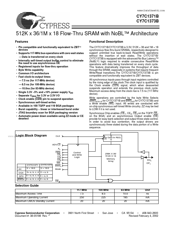
The CY7C1371B/CY7C1373B is 3.3V, 512K × 36 and 1M × 18 synchronous flow-thru burst SRAMs, respectively designed to support unlimited true back-to-back Read/Write operations without the insertion of wait states.
| Part number | CY7C1371B |
|---|---|
| Manufacturer | Cypress (Infineon) |
| File Size | 932.55 KB |
| Description | (CY7C1371B / CY7C1373B) 512K x 36/1M x 18 Flow-Thru SRAM |
| Datasheet |
CY7C1371B Datasheet
|
|
|
|
| Part Number | Description | Manufacturer |
|---|---|---|
| CY7C1371C | 18-Mbit (512K x 36/1M x 18) Flow-Through SRAM with NoBL Architecture | Cypress |
| CY7C1371S | 18-Mbit (512K x 36) Flow-Through SRAM | Cypress |
| CY7C1370C | 512K x 36/1M x 18 Pipelined SRAM with NoBL Architecture | Cypress |
| CY7C1370CV25 | 512K x 36/1M x 18 Pipelined SRAM with NoBL Architecture | Cypress |
| CY7C1370D | 18-Mbit (512 K 횞 36/1 M 횞 18) Pipelined SRAM | Cypress |
| Part Number | Description |
|---|---|
| CY7C1371D | 18-Mbit (512 K x 36/1 M x 18) Flow-Through SRAM |
| CY7C1371DV25 | (CY7C1371DV25 / CY7C1373DV25) Flow-Through SRAM |
| CY7C1371KV33 | 18-Mbit (512K x 36/1M x 18) Flow-Through SRAM |
| CY7C1371KVE33 | 18-Mbit (512K x 36/1M x 18) Flow-Through SRAM |
| CY7C1370B | (CY7C1370B / CY7C1372B) 512K X 36/1M X 18 Pipelined SRAM |
The following content is an automatically extracted verbatim text from the original manufacturer datasheet and is provided for reference purposes only.