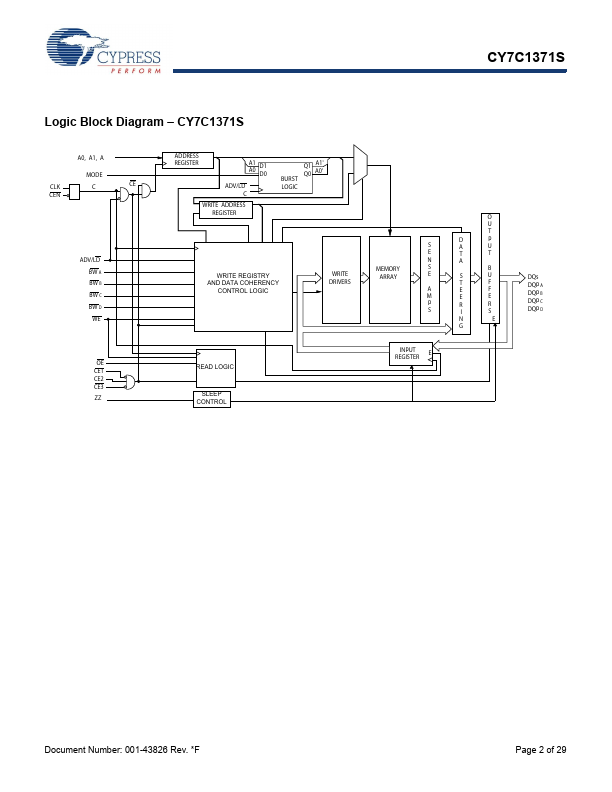
The CY7C1371S is a 3.3 V, 512K × 36 Synchronous flow through Burst SRAM designed specifically to support unlimited true back-to-back Read/Write operations with no wait state insertion.
Features
No Bus Latency (NoBL) architecture eliminates dead cycles between write and read cycles.
Supports up to 133-MHz bus operations with zero wait states.
Data is transferred on every clock.
Pin-compatible and functionally equivalent to ZBT™ devices.
Internally self-timed output buffer control to eliminate the need
to use OE.
CY7C1371KV33 - 18-Mbit (512K x 36/1M x 18) Flow-Through SRAM(Cypress Semiconductor)
CY7C1371KVE33 - 18-Mbit (512K x 36/1M x 18) Flow-Through SRAM(Cypress Semiconductor)
CY7C1370B - (CY7C1370B / CY7C1372B) 512K X 36/1M X 18 Pipelined SRAM(Cypress Semiconductor)
CY7C1370DV25 - 18-Mbit (512K x 36/1M x 18) Pipelined SRAM(Cypress Semiconductor)
CY7C1370KV25 - 18-Mbit (512K x 36/1M x 18) Pipelined SRAM(Cypress Semiconductor)
CY7C1370KV33 - 18-Mbit (512K x 36/1M x 18) Pipelined SRAM(Cypress Semiconductor)
CY7C1370KVE33 - 18-Mbit (512K x 36/1M x 18) Pipelined SRAM(Cypress Semiconductor)
Other Datasheets by Cypress
CY7C1371C- 18-Mbit (512K x 36/1M x 18) Flow-Through SRAM with NoBL Architecture
CY7C1370C- 512K x 36/1M x 18 Pipelined SRAM with NoBL Architecture
CY7C1370CV25- 512K x 36/1M x 18 Pipelined SRAM with NoBL Architecture
CY7C1370D- 18-Mbit (512 K 횞 36/1 M 횞 18) Pipelined SRAM
CY7C1372C- 512K x 36/1M x 18 Pipelined SRAM with NoBL Architecture
CY7C1372CV25- 512K x 36/1M x 18 Pipelined SRAM with NoBL Architecture
CY7C1372D- 18-Mbit (512 K 횞 36/1 M 횞 18) Pipelined SRAM
CY7C1373C- 18-Mbit (512K x 36/1M x 18) Flow-Through SRAM with NoBL Architecture
Full PDF Text Transcription
Click to expand full text
CY7C1371S
18-Mbit (512K × 36) Flow-Through SRAM with NoBL™ Architecture
18-Mbit (512K × 36) Flow-Through SRAM with NoBL™ Architecture
Features
■ No Bus Latency (NoBL) architecture eliminates dead cycles between write and read cycles
■ Supports up to 133-MHz bus operations with zero wait states ■ Data is transferred on every clock ■ Pin-compatible and functionally equivalent to ZBT™ devices ■ Internally self-timed output buffer control to eliminate the need
to use OE ■ Registered inputs for flow through operation ■ Byte Write capability ■ 3.3 V/2.5 V I/O power supply (VDDQ) ■ Fast clock-to-output times
❐ 6.
 CY7C1371S Datasheet