HYB39S16160CT-6 Overview
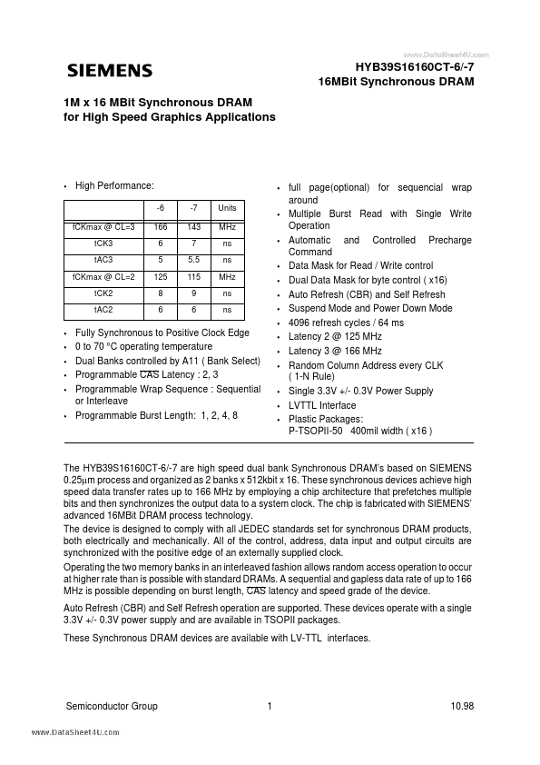
Key Specifications
Operating Voltage: 3.3 V
Max Voltage (typical range): 3.6 V
Min Voltage (typical range): 3 V
Max Frequency: 166 MHz
Key Features
- High Performance
- 6 fCKmax @ CL=3 tCK3 tAC3 fCKmax @ CL=2 tCK2 tAC2 166 6 5 125 8 6 -7 143 7 5.5 115 9 6 Units MHz ns ns MHz ns ns