Download the K7R321882C datasheet PDF.
This datasheet also covers the K7R320982C variant, as both devices belong to the same (k7r32xx82c) qdr ii b2 sram family and are provided as variant models within a single manufacturer datasheet.
Description
Input Clock Input Clock for Output Data Output Echo Clock DLL Disable when low Address Inputs Data Inputs 1 NOTE
Q0-35 W R BW0, BW1,BW2, BW3 VREF ZQ VDD VDDQ VSS TMS TDI TCK TDO NC
Data Outputs Write Control Pin, active when low Read Control Pin, active when low Block Write Control Pin, active whe
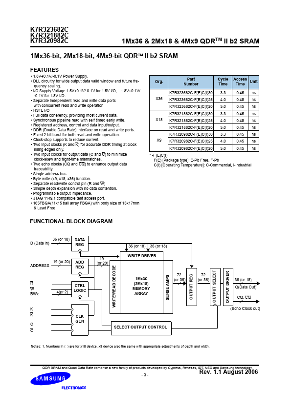
Features
- 1.8V+0.1V/-0.1V Power Supply.
- DLL circuitry for wide output data valid window and future frequency scaling.
- I/O Supply Voltage 1.5V+0.1V/-0.1V for 1.5V I/O, 1.8V+0.1V/ -0.1V for 1.8V I/O.
- Separate independent read and write data ports with concurrent read and write operation.
- HSTL I/O.
- Full data coherency, providing most current data.
- Synchronous pipeline read with self timed early write.
- Registered address, control an.
 K7R321882C Datasheet