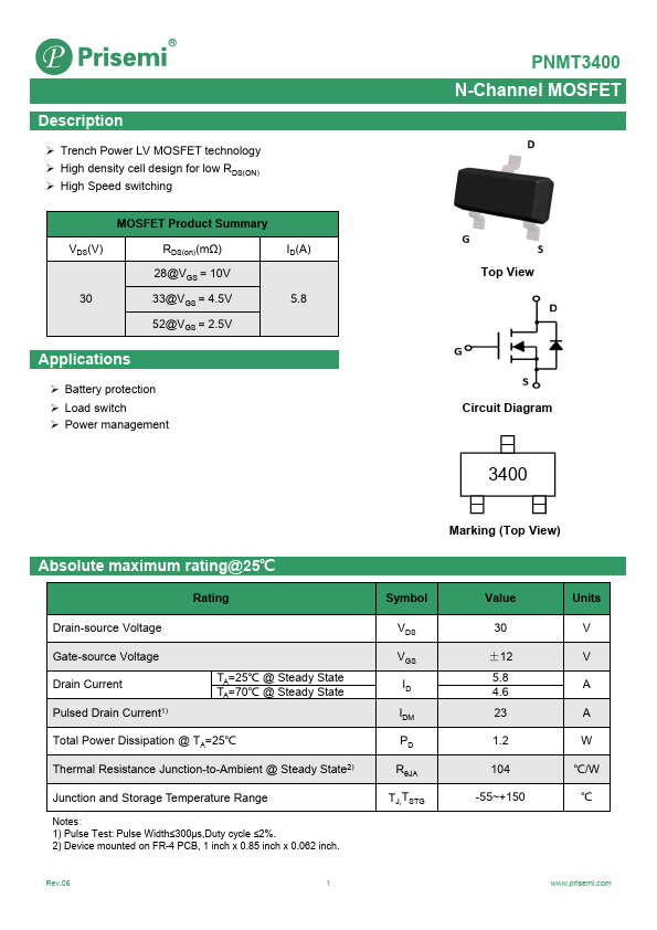
PNMT3400 Description
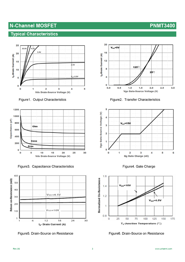
Pulse Width≤300μs,Duty cycle ≤2%. 2) Device mounted on FR-4 PCB, 1 inch x 0.85 inch x 0.062 inch. N-Channel MOSFET Typical Characteristics PNMT3400 Rev.06 3 .prisemi.
PNMT3400 is N-Channel MOSFET manufactured by Prisemi.
| Part Number | Description |
|---|---|
| PNMT30V2A | N-Channel MOSFET |
| PNMT100V2 | N-Channel MOSFET |
| PNMT20V2A | N-Channel MOSFET |
| PNMT20V2SA | N-Channel MOSFET |
| PNMT20V6 | N-Channel MOSFET |
Pulse Width≤300μs,Duty cycle ≤2%. 2) Device mounted on FR-4 PCB, 1 inch x 0.85 inch x 0.062 inch. N-Channel MOSFET Typical Characteristics PNMT3400 Rev.06 3 .prisemi.