PNMT20V2SA
Description
The MOSFET provide the best bination of fast switching , low on-resistance and cost-effectiveness.
- Trench Power LV MOSFET technology
- Voltage controlled small signal switch
- Low input Capacitance
- Fast Switching Speed
- Low Input / Output Leakage
MOSFET Product Summary
VDS(V) 20
RDS(on)(mΩ) 50@VGS=4.5V
ID(A) 3.0
PNMT20V2SA N-Channel MOSFET
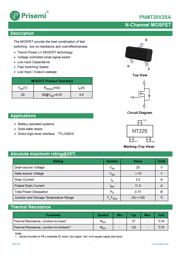
Top View
Applications
- Battery operated systems
- Solid-state relays
- Direct logic-level interface:TTL/CMOS
Circuit Diagram
D(3)
NT22S
Absolute maximum rating@25℃
Rating Drain-source Voltage Gate-source Voltage Drain Current Pulsed Drain Current Total Power Dissipation Junction and Storage Temperature Range
G(1)
S(2)
Marking (Top View)
Symbol VDS VGS ID IDM PD
TJ,TSTG
Value 20
±10 3.0 11.5 0.75 -55~+150
Units V V A A W ℃
Thermal Resistance
Parameter
Symbol
Min
Typ
Max
Unit
Thermal Resistance, Junction-to-Case1) Thermal Resistance, Junction-to-Ambient1)...