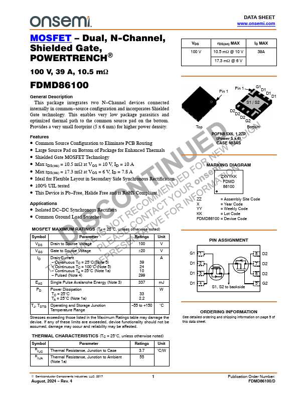
Description
This package integrates two N
Channel devices connected
internally in common
source configuration and incorporates Shielded Gate technology.
This enables very low package parasitics and optimized thermal path to the common source pad on the bottom.
Features
- Common Source Configuration to Eliminate PCB Routing.
- Large Source Pad on Bottom of Package for Enhanced Thermals.
- Shielded Gate MOSFET Technology.
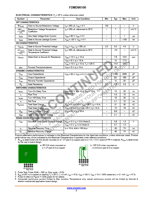
- Max rDS(on) = 10.5 mW at VGS = 10 V, ID = 10 A.
- Max rDS(on) = 17.3 mW at VGS = 6 V, ID = 7.8 A.
- Ideal for Flexible Layout in Secondary Side Synchronous Rectification.
- 100% UIL tested.
- This Device is Pb.
- Free, Halide Free and is RoHS Compliant.
 FDMD86100 Datasheet