LD7271
LD7271 is Smart Photoflash Capacitor Charger manufactured by Leadtrend.
Description
The LD7271 is an ide al charge control IC for flash un its, featuring i nternal s oft st art, adjustable ch arging curre nt and o utput vol tage. It provid es a charg ing algor ithm to speed up the charging with higher efficiency. The LD7271 can o perate i n des ired c onstant peak c urrent of ei ght different levels bet ween 0.6A and 1.3A, b y clocking th e CHARGE pin. The LD7271 i s availa ble in a space-savi ng W DFN-8L 2mm x 2mm package and is ideal for DSC flash unit.
Features
- -
- -
- - 1.8V~6V Battery Voltage Range Adjustable Output Voltage Adjustable Input Current Integrated 47V Power MOS False Triggering Prevention Start Efficiency Output Voltage Overcharge Protection
- Soft
- High
Applications
- DSC Flash Unit Phone
- Camera g Patented
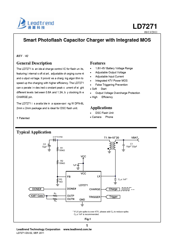
Typical Application
D1/FT01P80
C2 72μF
R1 130kΩ
C1 10μF~22μF
R2 130kΩ
1μF
R3 1kΩ
CS ≤ 1n F-
RP RN
- If LX pin spike is over 47V, please add CS to reduce spike. CS ≤ 1n F is remended.
Fig.1
Leadtrend Technology Corporation
LD7271-DS-02, SEP. 2011 http://..
.leadtrend..tw
Pin Configuration
WDFN-8 (2mm x 2mm) TRIGGER CHARGE
LX a: : p: Y: W: T: T a P Yw T
1 2 3 4
DONE#
Ordering Information
Part number LD7271GDDW Package WDFN-8L 2x2 Green Package Top Mark a P Shipping 2500 /tape & reel
The LD7271 is green packaged.
Pin Descriptions
PIN N 1 DONE# 2 3 4 5 6 7 8 Exposed Metal Pad OUTN OUTP VCC FB CHARGE TRIGGER LX GND AME FUNCTION Charge Done Indicator. DONE# is a push-pull drain output that pulls low when CHARGE is high and the circuit has finished charging the output capacitor. IGBT driver sink output pin. IGBT driver source output pin. Input power of IC. Bypass with a 1μF ceramic capacitor close to IC GND. Output voltage feedback Charging on/off control. Trigger on/off control. NMOS drain pin. Connect to transformer primary as shown in Fig.1. IC GND. Exposed pad should be soldered to PCB board with a larger...