IS61NVVP25672 Description
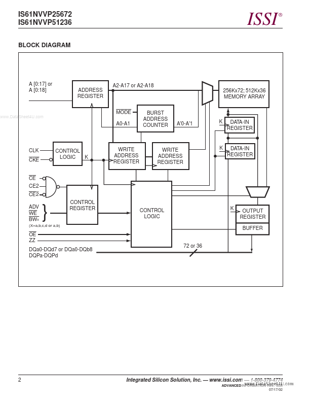
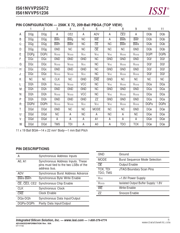
® Byte Write Control Single R/W (Read/Write) control pin Clock controlled, registered address, data and control Interleaved or linear burst sequence control using MODE input Power Down mode mon data inputs and data outputs CKE pin to enable clock and suspend operation JEDEC 119-ball PBGA (x36) and 209-ball (x72) PBGA packages Single +1.8V (± 5%) power supply JTAG Boundary Scan Industrial temperature available The 16...
IS61NVVP25672 Key Features
- 100 percent bus utilization
- No wait cycles between Read and Write
- Internal self-timed write cycle
- Individual
- Single R/W (Read/Write) control pin
- Clock controlled, registered address, data and control
- Interleaved or linear burst sequence control using MODE input
- Power Down mode
- mon data inputs and data outputs
- CKE pin to enable clock and suspend operation