CY7C1482BV33 Key Features
- Functional Description
- Selection Guide
- 198 Champion Court
- San Jose, CA 95134-1709
- 408-943-2600 Revised March 05, 2008
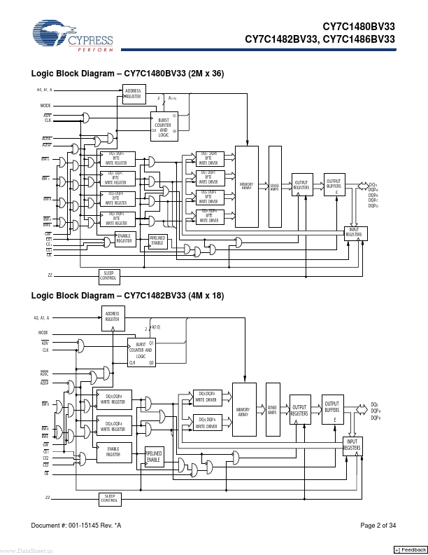
- CY7C1480BV33 (2M x 36)

| Part Number | Description |
|---|---|
| CY7C1482BV25 | (CY7C148xBV25) 72-Mbit (2M x 36/4M x 18/1M x 72) Pipelined Sync SRAM |
| CY7C1482V33 | (CY7C1480V33 / CY7C1482V33 / CY7C1486V33) 72-Mbit (2M x 36/4M x 18/1M x 72) Pipelined Sync SRAM |
| CY7C148 | (CY7C148 / CY7C149) 1K x 4 Static RAM |
| CY7C1480BV25 | 72-Mbit (2M x 36/4M x 18/1M x 72) Pipelined Sync SRAM |
| CY7C1480BV33 | (CY7C148xBV33) 72-Mbit (2M x 36/4M x 18/1M x 72) Pipelined Sync SRAM |