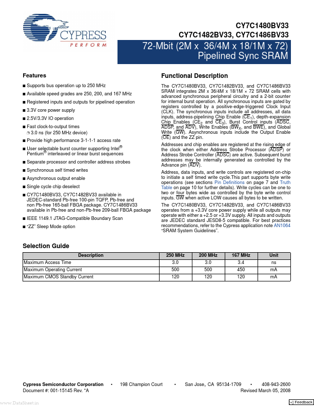
| Part | CY7C1480BV33 |
|---|---|
| Description | 72-Mbit (2M x 36/4M x 18/1M x 72) Pipelined Sync SRAM |
| Manufacturer | Cypress |
| Size | 0.97 MB |
Pricing from 109.44192 USD, available from Avnet and Rochester Electronics.
Price & Availability
| Seller | Inventory | Price Breaks | Buy |
|---|---|---|---|
| Avnet | 541 | 7+ : 109.44192 USD 14+ : 107.90912 USD 28+ : 106.37632 USD 56+ : 104.84352 USD |
View Offer |
| Avnet | 0 | 210+ : 172.92352 USD 420+ : 166.18624 USD 840+ : 159.44896 USD 1680+ : 152.71168 USD |
View Offer |
Similar Parts
| Part Number | Manufacturer | Description |
|---|---|---|
| LH52256C-10LL | Sharp Corporation | 256K SRAM |
| HM628512 | Hitachi Semiconductor | 4 M SRAM (512-kword x 8-bit) |
| HY62256A | Hyundai | 32K x 8-Bit CMOS SRAM |
