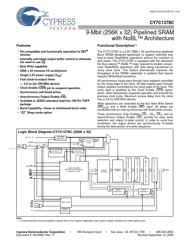
Datasheet4U Logo Datasheet4U.com

CY7C1378C - 9-Mbit (256K x 32) Pipelined SRAM

Description

The CY7C1378C is a 3.3V, 256K x 32 synchronous-pipelined Burst SRAM designed specifically to support unlimited true back-to-back Read/Write operations without the insertion of wait states.

Features

  • Pin-compatible and functionally equivalent to ZBT® devices.
  • Internally self-timed output buffer control to eliminate the need to use OE.
  • Byte Write capability.
  • 256K x 32 common I/O architecture.
  • Single 3.3V power supply (VDD).
  • Fast clock-to-output times.
  • 2.8 ns (for 250-MHz device).
  • Clock Enable (CEN) pin to suspend operation.
  • Synchronous self-timed writes.
  • Asynchronous Output Enable (OE).
  • Availab.

📥 Download Datasheet

Datasheet preview – CY7C1378C

Datasheet Details

Part number CY7C1378C
Manufacturer Cypress Semiconductor
File Size 350.24 KB
Description 9-Mbit (256K x 32) Pipelined SRAM
Datasheet download datasheet CY7C1378C Datasheet
Additional preview pages of the CY7C1378C datasheet.
Other Datasheets by Cypress Semiconductor

Full PDF Text Transcription

Click to expand full text
CY7C1378C 9-Mbit (256K x 32) Pipelined SRAM with NoBL™ Architecture Features • Pin-compatible and functionally equivalent to ZBT® devices • Internally self-timed output buffer control to eliminate the need to use OE • Byte Write capability • 256K x 32 common I/O architecture • Single 3.3V power supply (VDD) • Fast clock-to-output times — 2.8 ns (for 250-MHz device) • Clock Enable (CEN) pin to suspend operation • Synchronous self-timed writes • Asynchronous Output Enable (OE) • Available in JEDEC-standard lead-free 100-Pin TQFP package • Burst Capability—linear or interleaved burst order • “ZZ” Sleep mode option Functional Description[1] The CY7C1378C is a 3.
Published: |