CY7C1371B - (CY7C1371B / CY7C1373B) 512K x 36/1M x 18 Flow-Thru SRAM
Datasheet Summary
Description
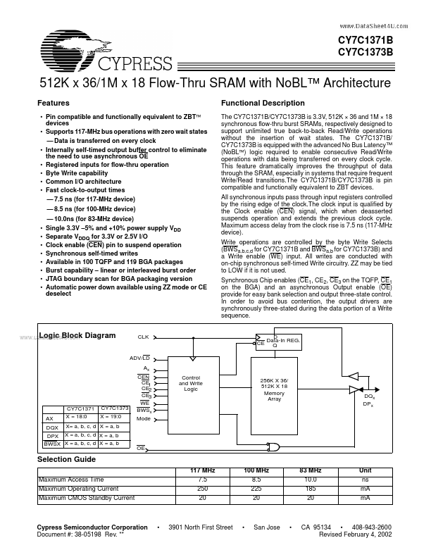
The CY7C1371B/CY7C1373B is 3.3V, 512K × 36 and 1M × 18 synchronous flow-thru burst SRAMs, respectively designed to support unlimited true back-to-back Read/Write operations without the insertion of wait states.
Features
Pin compatible and functionally equivalent to ZBT devices.
Supports 117-MHz bus operations with zero wait states.
Data is transferred on every clock.
Internally self-timed output buffer control to eliminate the need to use asynchronous OE.
CY7C1371KV33- 18-Mbit (512K x 36/1M x 18) Flow-Through SRAM
CY7C1371KVE33- 18-Mbit (512K x 36/1M x 18) Flow-Through SRAM
CY7C1370B- (CY7C1370B / CY7C1372B) 512K X 36/1M X 18 Pipelined SRAM
CY7C1370DV25- 18-Mbit (512K x 36/1M x 18) Pipelined SRAM
CY7C1370KV25- 18-Mbit (512K x 36/1M x 18) Pipelined SRAM
CY7C1370KV33- 18-Mbit (512K x 36/1M x 18) Pipelined SRAM
Full PDF Text Transcription
Click to expand full text
73B
CY7C1371B CY7C1373B
512K x 36/1M x 18 Flow-Thru SRAM with NoBL™ Architecture
Features
• Pin compatible and functionally equivalent to ZBT devices • Supports 117-MHz bus operations with zero wait states — Data is transferred on every clock • Internally self-timed output buffer control to eliminate the need to use asynchronous OE • Registered inputs for flow-thru operation • Byte Write capability • Common I/O architecture • Fast clock-to-output times — 7.5 ns (for 117-MHz device) — 8.5 ns (for 100-MHz device) • • • • • • • • — 10.0ns (for 83-MHz device) Single 3.3V –5% and +10% power supply VDD Separate VDDQ for 3.3V or 2.
 CY7C1371B Datasheet