CY7C1338B
CY7C1338B is 128K x 32 Synchronous-Flow-Through 3.3V Cache RAM manufactured by Cypress.
Features
- Supports 117-MHz microprocessor cache systems with zero wait states
- 128K by 32 mon I/O
- Fast clock-to-output times
- 7.5 ns (117-MHz version)
- Two-bit wraparound counter supporting either interleaved or linear burst sequence
- Separate processor and controller address strobes provide direct interface with the processor and external .. cache controller
- Synchronous self-timed write
- Asynchronous output enable
- 3.3V/ 2.5V I/Os
- JEDEC-standard pinout
- 100-pin TQFP packaging
- ZZ “sleep” mode
- Available in mercial and Industrial Temperatures
Functional Description
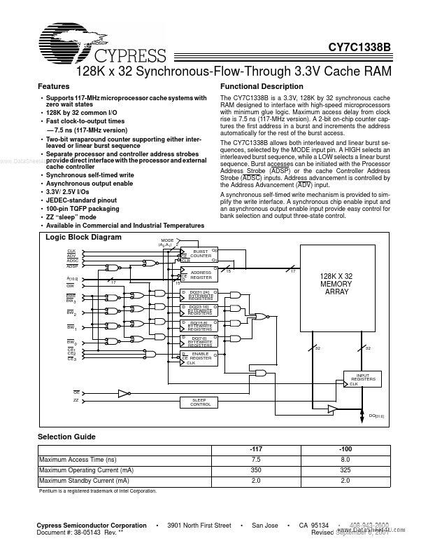
The CY7C1338B is a 3.3V, 128K by 32 synchronous cache RAM designed to interface with high-speed microprocessors with minimum glue logic. Maximum access delay from clock rise is 7.5 ns (117-MHz version). A 2-bit on-chip counter captures the first address in a burst and increments the address automatically for the rest of the burst access. The CY7C1338B allows both interleaved and linear burst sequences, selected by the MODE input pin. A HIGH selects an interleaved burst sequence, while a LOW selects a linear burst sequence. Burst accesses can be initiated with the Processor Address Strobe (ADSP) or the cache Controller Address Strobe (ADSC) inputs. Address advancement is controlled by the Address Advancement (ADV) input. A synchronous self-timed write mechanism is provided to simplify the write interface. A synchronous chip enable input and an asynchronous output enable input provide easy control for bank selection and output three-state control.
Logic Block Diagram
CLK ADV ADSC ADSP A[16:0] GW BWE BW 3 BW 2 BW 1
MODE (A0,A1) 2 BURST Q0 CE COUNTER Q1 CLR Q ADDRESS CE REGISTER D D DQ[31:24] Q BYTEWRITE REGISTERS 15 17
128K X 32 MEMORY ARRAY
D DQ[23:16] Q BYTEWRITE REGISTERS D Q DQ[15:8] BYTEWRITE REGISTERS Q DQ[7:0] BYTEWRITE REGISTERS
D BW 0 CE1 CE2 CE 3
D ENABLE Q CE REGISTER CLK INPUT REGISTERS CLK
OE ZZ SLEEP CONTROL DQ[31:0]
Selection Guide
-117 Maximum Access...