Part number:
CEU1012L
Manufacturer:
CET
File Size:
417.68 KB
Description:
N-channel mosfet.
CEU1012L Features
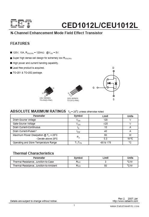
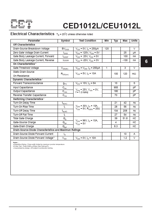
* 120V, 10A, RDS(ON) = 120mΩ @VGS = 5V. Super high dense cell design for extremely low RDS(ON). High power and current handing capability. Lead free product is acquired. TO-251 & TO-252 package. CED1012L/CEU1012L D D G S CEU SERIES TO-252(D-PAK) G D G S CED SERIES TO-251(I-PAK) S ABSOLUTE MAXIMU
Datasheet Details
CEU1012L
CET
417.68 KB
N-channel mosfet.
📁 Related Datasheet
CEU1012 N-Channel MOSFET (CET)
CEU101J Disc Ceramic Capacitors (Mallory)
CEU100D Disc Ceramic Capacitors (Mallory)
CEU10P10 P-Channel MOSFET (Chino-Excel Technology)
CEU110P03 P-Channel MOSFET (CET)
CEU1185 N-Channel MOSFET (CET)
CEU11P20 P-Channel MOSFET (CET)
CEU121J Disc Ceramic Capacitors (Mallory)
CEU1012L Distributor