CEU11P20 Description
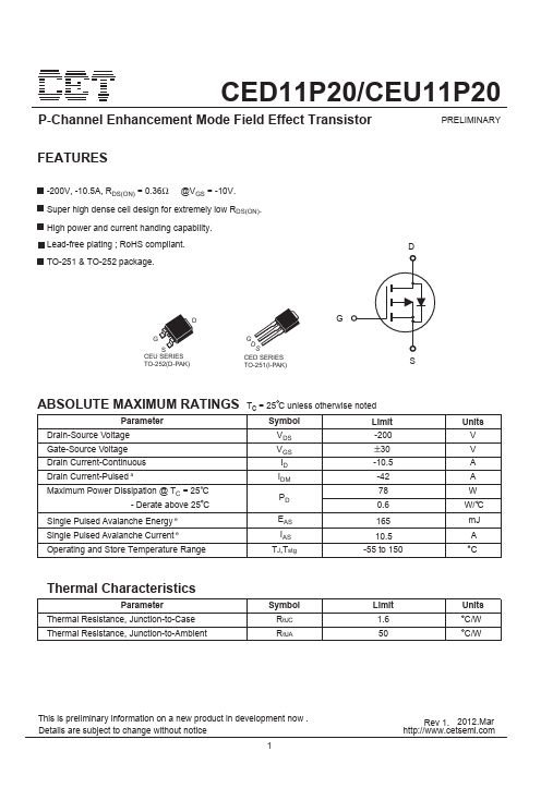
CED11P20/CEU11P20 P-Channel Enhancement Mode Field Effect Transistor PRELIMINARY.
CEU11P20 Key Features
- 200V, -10.5A, RDS(ON) = 0.36Ω @VGS = -10V. Super high dense cell design for extremely low RDS(ON). High power and curren
CEU11P20 is P-Channel MOSFET manufactured by CET.
| Part Number | Description |
|---|---|
| CEU110P03 | P-Channel MOSFET |
| CEU1185 | N-Channel MOSFET |
| CEU1012 | N-Channel MOSFET |
| CEU1012L | N-Channel MOSFET |
| CEU12N10 | N-Channel MOSFET |
CED11P20/CEU11P20 P-Channel Enhancement Mode Field Effect Transistor PRELIMINARY.