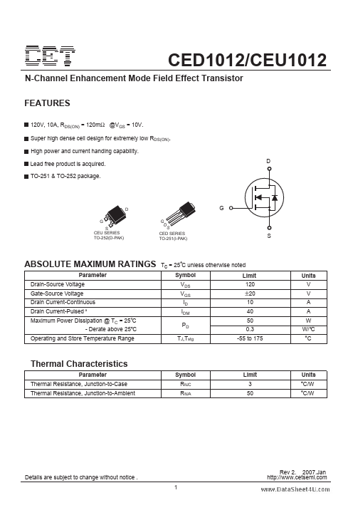
CED1012/CEU1012
Electrical Characteristics Tc = 25 C unless otherwise noted
Parameter
Symbol
Test Condition
Off Characteristics
Drain-Source Breakdown Voltage
Zero Gate Voltage Drain Current
Gate Body Leakage Current, Forward
Gate Body Leakage Current, Reverse
On Characteristics b
BVDSS
IDSS
IGSSF
IGSSR
VGS = 0V, ID = 250µA
VDS = 120V, VGS = 0V
VGS = 20V, VDS = 0V
VGS = -20V, VDS = 0V
Gate Threshold Voltage
Static Drain-Source
On-Resistance
VGS(th)
RDS(on)
VGS = VDS, ID = 250µA
VGS = 10V, ID = 10A
Dynamic Characteristics c
Forward Transconductance
gFS VDS = 10V, ID = 5A
Input Capacitance
Output Capacitance
Reverse Transfer Capacitance
Switching Characteristics c
Ciss
Coss
Crss
VDS = 25V, VGS = 0V,
f = 1.0 MHz
Turn-On Delay Time
Turn-On Rise Time
Turn-Off Delay Time
td(on)
tr
td(off)
VDD = 30V, ID = 15A,
VGS = 10V, RGEN = 20Ω
Turn-Off Fall Time
tf
Total Gate Charge
Gate-Source Charge
Gate-Drain Charge
Qg
Qgs
VDS = 96V, ID = 10A,
VGS = 10V
Qgd
Drain-Source Diode Characteristics and Maximun Ratings
Drain-Source Diode Forward Current
Drain-Source Diode Forward Voltage b
IS
VSD
VGS = 0V, IS = 10A
Notes :
a.Repetitive Rating : Pulse width limited by maximum junction temperature.
b.Pulse Test : Pulse Width < 300µs, Duty Cycle < 2%.
c.Guaranteed by design, not subject to production testing.
Min
120
2
Typ
100
5
690
195
85
15
10
37
14
23.6
3.8
9
Max Units
25
100
-100
V
µA
nA
nA
4V
120 mΩ
S
pF
pF
pF
30 ns
20 ns
74 ns
28 ns
31.4 nC
nC
nC
10 A
1.2 V
6
2