Datasheet Details
| Part number | 74ALVCH16821DGG |
|---|---|
| Manufacturer | nexperia |
| File Size | 188.24 KB |
| Description | 20-bit bus-interface D-type flip-flop |
| Datasheet |
 74ALVCH16821DGG Datasheet 74ALVCH16821DGG Datasheet
|
|
|
Download the 74ALVCH16821DGG datasheet PDF. This datasheet also covers the 74ALVCH16821 variant, as both devices belong to the same 20-bit bus-interface d-type flip-flop family and are provided as variant models within a single manufacturer datasheet.
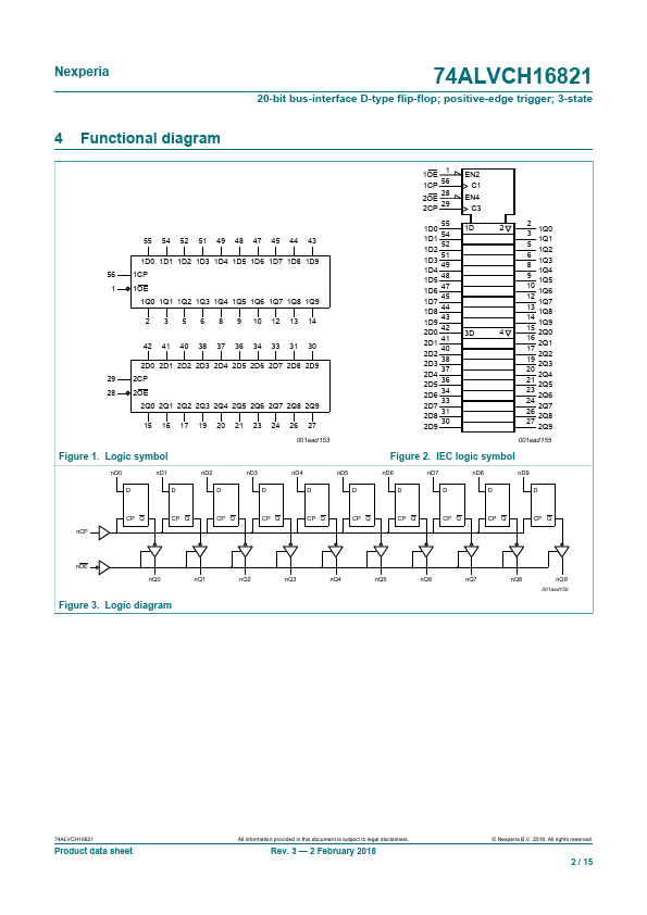
The 74ALVCH16821 has two 10-bit, edge triggered registers, with each register coupled to a 3-state output buffer.
The two sections of each register are controlled independently by the clock (nCP) and output enable (nOE) control gates.
Each register is fully edge triggered.
| Part number | 74ALVCH16821DGG |
|---|---|
| Manufacturer | nexperia |
| File Size | 188.24 KB |
| Description | 20-bit bus-interface D-type flip-flop |
| Datasheet |
74ALVCH16821DGG Datasheet
|
|
|
|
| Part Number | Description | Manufacturer |
|---|---|---|
| 74ALVCH16821 | 20-bit bus-interface D-type flip-flop | NXP |
| 74ALVCH16823 | 18-bit bus-interface D-type flip-flop | NXP |
| 74ALVCH16825 | 18-bit buffer/driver | NXP |
| 74ALVCH16827 | 20-bit buffer/line driver | NXP |
| 74ALVCH16841 | 20-bit bus interface D-type latch | NXP |
| Part Number | Description |
|---|---|
| 74ALVCH16821 | 20-bit bus-interface D-type flip-flop |
| 74ALVCH16823 | 18-bit bus-interface D-type flip-flop |
| 74ALVCH16823DGG | 18-bit bus-interface D-type flip-flop |
| 74ALVCH16825 | 18-bit buffer/driver |
| 74ALVCH16825DGG | 18-bit buffer/driver |