Datasheet Details
| Part number | 74AHCT374-Q100 |
|---|---|
| Manufacturer | nexperia |
| File Size | 788.60 KB |
| Description | Octal D-type flip-flop |
| Datasheet |
 74AHCT374-Q100 Datasheet 74AHCT374-Q100 Datasheet
|
|
|
Download the 74AHCT374-Q100 datasheet PDF. This datasheet also covers the 74AHC374-Q100 variant, as both devices belong to the same octal d-type flip-flop family and are provided as variant models within a single manufacturer datasheet.
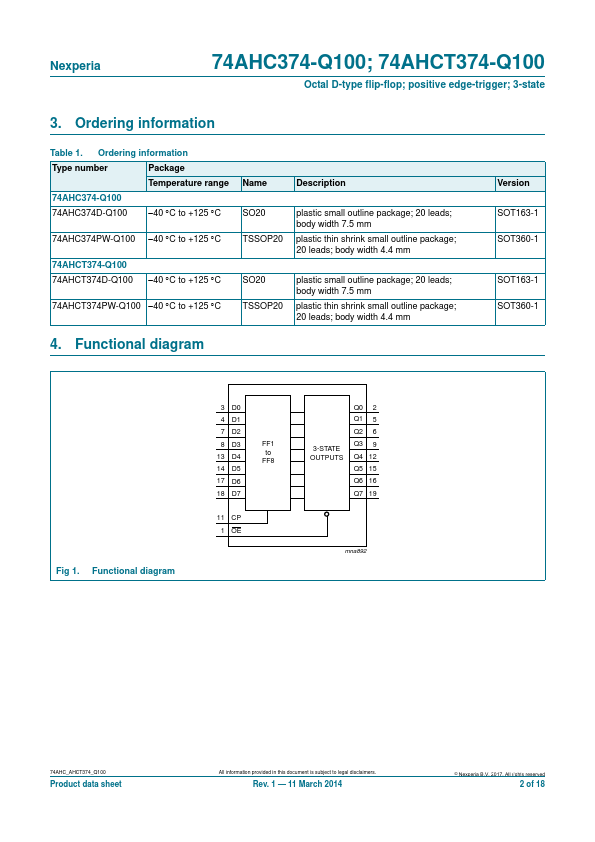
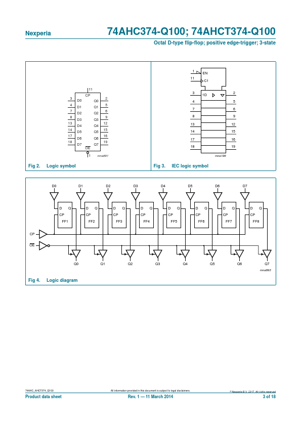
The 74AHC374-Q100; 74AHCT374-Q100 is a high-speed Si-gate CMOS device and is pin compatible with Low-power Schottky TTL (LSTTL).
It is specified in compliance with JEDEC standard No.
7-A.
| Part number | 74AHCT374-Q100 |
|---|---|
| Manufacturer | nexperia |
| File Size | 788.60 KB |
| Description | Octal D-type flip-flop |
| Datasheet |
74AHCT374-Q100 Datasheet
|
|
|
|
| Part Number | Description | Manufacturer |
|---|---|---|
| 74AHCT374 | Octal D-type flip-flop | NXP |
| 74AHCT373 | Octal D-type transparent latch | NXP |
| 74AHCT30 | 8-input NAND gate | NXP |
| 74AHCT32 | Quad 2-input OR gate | NXP |
| 74AHCT32 | QUADRUPLE 2-INPUT OR GATE | Diodes |
| Part Number | Description |
|---|---|
| 74AHCT374 | Octal D-type flip-flop |
| 74AHCT374D | Octal D-type flip-flop |
| 74AHCT374PW | Octal D-type flip-flop |
| 74AHCT377 | Octal D-type flip-flop |
| 74AHCT377-Q100 | Octal D-type flip-flop |