Click to expand full text
Product Folder
Order Now
Technical Documents
Tools & Software
Support & Community
SN74LVC2G125
SCES204Q – APRIL 1999 – REVISED MARCH 2017
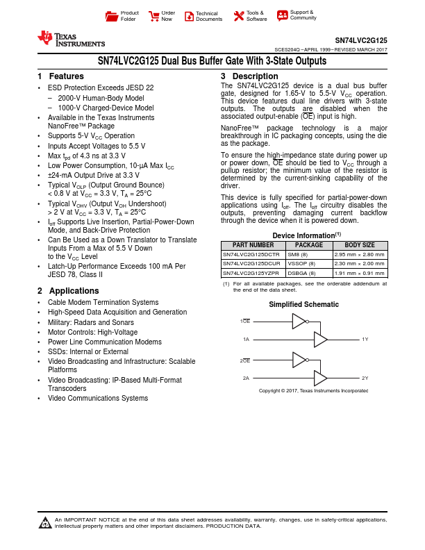
SN74LVC2G125 Dual Bus Buffer Gate With 3-State Outputs
1 Features
•1 ESD Protection Exceeds JESD 22 – 2000-V Human-Body Model – 1000-V Charged-Device Model
• Available in the Texas Instruments NanoFree™ Package
• Supports 5-V VCC Operation • Inputs Accept Voltages to 5.5 V • Max tpd of 4.3 ns at 3.3 V • Low Power Consumption, 10-µA Max ICC • ±24-mA Output Drive at 3.3 V • Typical VOLP (Output Ground Bounce)
< 0.8 V at VCC = 3.3 V, TA = 25°C • Typical VOHV (Output VOH Undershoot)
> 2 V at VCC = 3.
 SN74LVC2G125 Datasheet