Datasheet Details
| Part number | SN74LV126A |
|---|---|
| Manufacturer | Texas Instruments |
| File Size | 1.02 MB |
| Description | Quadruple Bus Buffer Gate |
| Datasheet |
 SN74LV126A Datasheet SN74LV126A Datasheet
|
|
|
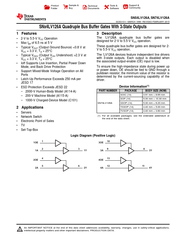
The ‘LV126A quadruple bus buffer gates are designed for 2-V to 5.5-V VCC operation.
These quadruple bus buffer gates are designed for 2V to 5.5-V VCC operation.
The ’LV126A devices feature independent line drivers with 3-state outputs.
| Part number | SN74LV126A |
|---|---|
| Manufacturer | Texas Instruments |
| File Size | 1.02 MB |
| Description | Quadruple Bus Buffer Gate |
| Datasheet |
SN74LV126A Datasheet
|
|
|
|
| Part Number | Description | Manufacturer |
|---|---|---|
| SN74LVC1G125 | high performance non-inverting buffer | UMW |
| SN74LVC1G34 | Single buffer | UMW |
| SN74L71 | AND-Gate R-S Master-Slave F-F | National Semiconductor |
| SN74L74N | Dual D-Type Flip-Flop | ETC |
| SN74LS00 | QUAD 2-INPUT NAND GATE | Motorola |
| Part Number | Description |
|---|---|
| SN74LV123A | Dual Retriggerable Monostable Multivibrators |
| SN74LV123A-EP | Dual Retriggerable Monostable Multivibrators |
| SN74LV123A-Q1 | Dual Retriggerable Monostable Multivibrators |
| SN74LV125A | Quadruple Bus Buffer Gates |
| SN74LV125A-Q1 | Quadruple Bus Buffer Gates |