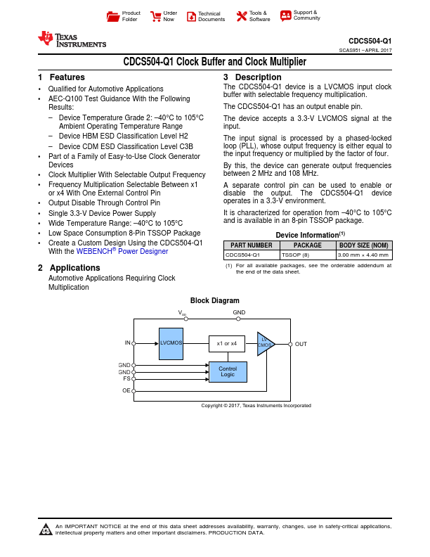
Datasheet4U Logo Datasheet4U.com

CDCS504-Q1 - Clock Buffer and Clock Multiplier

Datasheet Summary

Description

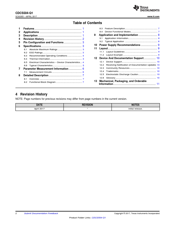
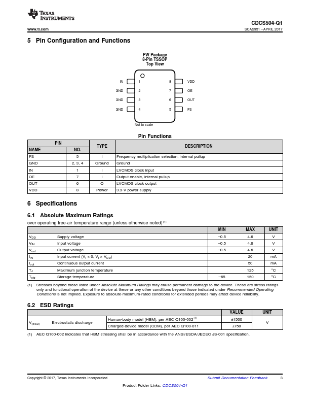
The CDCS504-Q1 device is a LVCMOS input clock buffer with selectable frequency multiplication.

The CDCS504-Q1 has an output enable pin.

The device accepts a 3.3-V LVCMOS signal at the input.

Features

  • 1 Qualified for Automotive.

📥 Download Datasheet

Datasheet preview – CDCS504-Q1

Datasheet Details

Part number CDCS504-Q1
Manufacturer Texas Instruments
File Size 633.88 KB
Description Clock Buffer and Clock Multiplier
Datasheet download datasheet CDCS504-Q1 Datasheet
Additional preview pages of the CDCS504-Q1 datasheet.
Other Datasheets by Texas Instruments

Full PDF Text Transcription

Click to expand full text
Product Folder Order Now Technical Documents Tools & Software Support & Community CDCS504-Q1 Clock Buffer and Clock Multiplier CDCS504-Q1 SCAS951 – APRIL 2017 1 Features •1 Qualified for Automotive Applications • AEC-Q100 Test Guidance With the Following Results: – Device Temperature Grade 2: –40°C to 105°C Ambient Operating Temperature Range – Device HBM ESD Classification Level H2 – Device CDM ESD Classification Level C3B • Part of a Family of Easy-to-Use Clock Generator Devices • Clock Multiplier With Selectable Output Frequency • Frequency Multiplication Selectable Between x1 or x4 With One External Control Pin • Output Disable Through Control Pin • Single 3.
Published: |