Datasheet4U Logo Datasheet4U.com

CDCS503 - Clock Buffer/Clock Multiplier

Datasheet Summary

Description

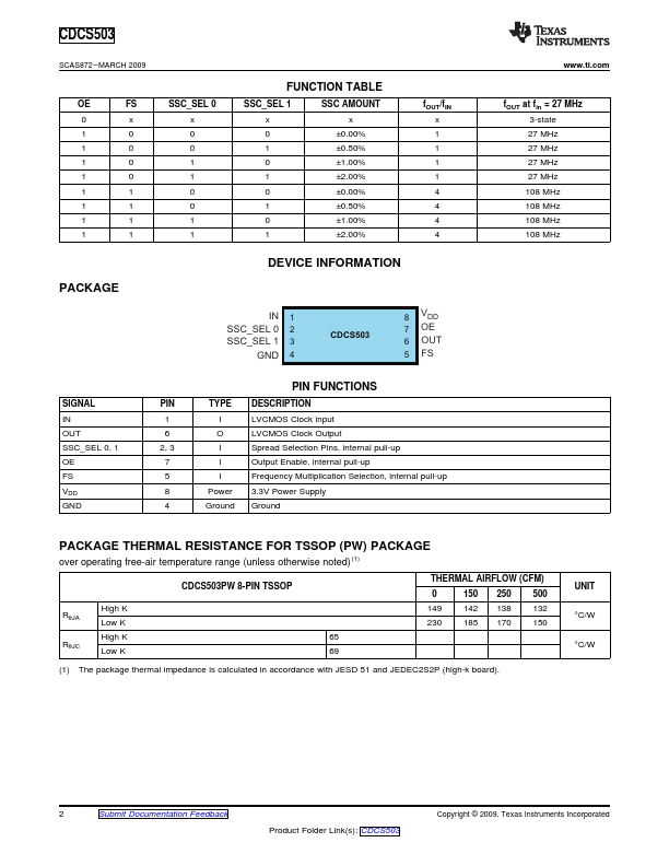
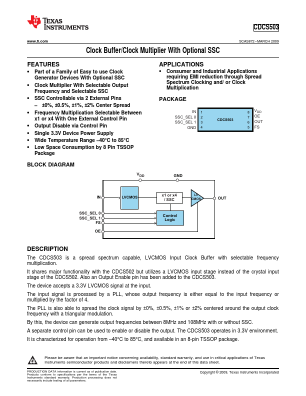
The CDCS503 is a spread spectrum capable, LVCMOS Input Clock Buffer with selectable frequency multiplication.

It shares major functionality with the CDCS502 but utilizes a LVCMOS input stage instead of the crystal input stage of the CDCS502.

Also an Output Enable pin has been added to the CDCS503.

Features

  • 1.
  • Part of a Family of Easy to use Clock Generator Devices With Optional SSC.
  • Clock Multiplier With Selectable Output Frequency and Selectable SSC.
  • SSC Controllable via 2 External Pins.
  • ±0%, ±0.5%, ±1%, ±2% Center Spread.
  • Frequency Multiplication Selectable Between x1 or x4 With One External Control Pin.
  • Output Disable via Control Pin.
  • Single 3.3V Device Power Supply.
  • Wide Temperature Range.
  • 40°C to 85°C.
  • Lo.

📥 Download Datasheet

Datasheet preview – CDCS503

Datasheet Details

Part number CDCS503
Manufacturer Texas Instruments
File Size 547.83 KB
Description Clock Buffer/Clock Multiplier
Datasheet download datasheet CDCS503 Datasheet
Additional preview pages of the CDCS503 datasheet.
Other Datasheets by Texas Instruments

Full PDF Text Transcription

Click to expand full text
CDCS503 www.ti.com .................................................................................................................................................................................................. SCAS872 – MARCH 2009 Clock Buffer/Clock Multiplier With Optional SSC FEATURES 1 • Part of a Family of Easy to use Clock Generator Devices With Optional SSC • Clock Multiplier With Selectable Output Frequency and Selectable SSC • SSC Controllable via 2 External Pins – ±0%, ±0.5%, ±1%, ±2% Center Spread • Frequency Multiplication Selectable Between x1 or x4 With One External Control Pin • Output Disable via Control Pin • Single 3.
Published: |