Datasheet4U Logo Datasheet4U.com

CDCS501 - SSC Clock Generator/Buffer

Datasheet Summary

Description

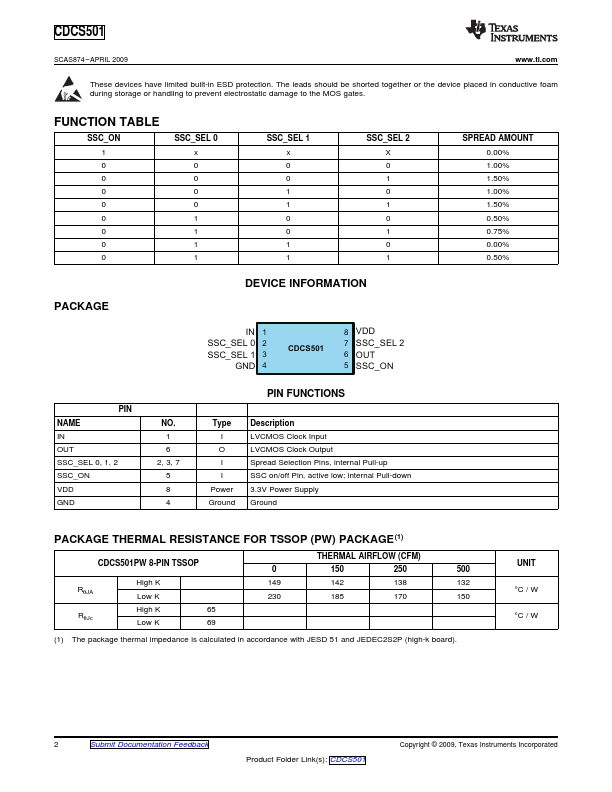
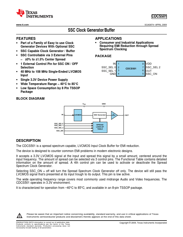
The CDCS501 is a spread spectrum capable, LVCMOS Input Clock Buffer for EMI reduction.

The device is designed to counter common EMI problems in modern electronic designs.

It accepts a 3.3V LVCMOS signal at the input and spread this signal by a small amount, centered around the input frequency.

Features

  • 1.
  • Part of a Family of Easy to use Clock Generator Devices With Optional SSC.
  • SSC Capable Clock Generator / Buffer.
  • SSC Controllable via 3 External Pins.
  • ±0% to ±1.5% Center Spread.
  • 1 External Control Pin for SSC ON / OFF Selection.
  • 40 MHz to 108 MHz Single-Ended LVCMOS Input.
  • Single 3.3V Device Power Supply.
  • Wide Temperature Range.
  • 40°C to 85°C.
  • Low Space Consumption by 8 Pin TSSOP Package BLOCK.

📥 Download Datasheet

Datasheet preview – CDCS501

Datasheet Details

Part number CDCS501
Manufacturer Texas Instruments
File Size 556.11 KB
Description SSC Clock Generator/Buffer
Datasheet download datasheet CDCS501 Datasheet
Additional preview pages of the CDCS501 datasheet.
Other Datasheets by Texas Instruments

Full PDF Text Transcription

Click to expand full text
CDCS501 www.ti.com..................................................................................................................................................................................................... SCAS874 – APRIL 2009 SSC Clock Generator/Buffer FEATURES 1 • Part of a Family of Easy to use Clock Generator Devices With Optional SSC • SSC Capable Clock Generator / Buffer • SSC Controllable via 3 External Pins – ±0% to ±1.5% Center Spread • 1 External Control Pin for SSC ON / OFF Selection • 40 MHz to 108 MHz Single-Ended LVCMOS Input • Single 3.
Published: |