Datasheet Details
| Part number | CDCLVD2102 |
|---|---|
| Manufacturer | Texas Instruments |
| File Size | 633.32 KB |
| Description | Dual 1:2 Low Additive Jitter LVDS Buffer |
| Datasheet |
 CDCLVD2102 Datasheet CDCLVD2102 Datasheet
|
|
|
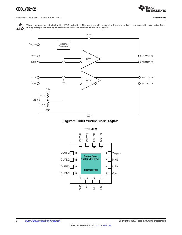
The CDCLVD2102 clock buffer distributes two clock inputs (IN0, IN1) to a total of 4 pairs of differential LVDS clock outputs (OUT0, OUT3).
Each buffer block consists of one input and 2 LVDS outputs.
The inputs can either be LVDS, LVPECL, or LVCMOS.
| Part number | CDCLVD2102 |
|---|---|
| Manufacturer | Texas Instruments |
| File Size | 633.32 KB |
| Description | Dual 1:2 Low Additive Jitter LVDS Buffer |
| Datasheet |
CDCLVD2102 Datasheet
|
|
|
|