Datasheet Details
| Part number | TC74HC4049AP |
|---|---|
| Manufacturer | Toshiba |
| File Size | 210.37 KB |
| Description | HEX BUFFER/CONVERTER |
| Datasheet |
 TC74HC4049AP Datasheet TC74HC4049AP Datasheet
|
|
|
2.
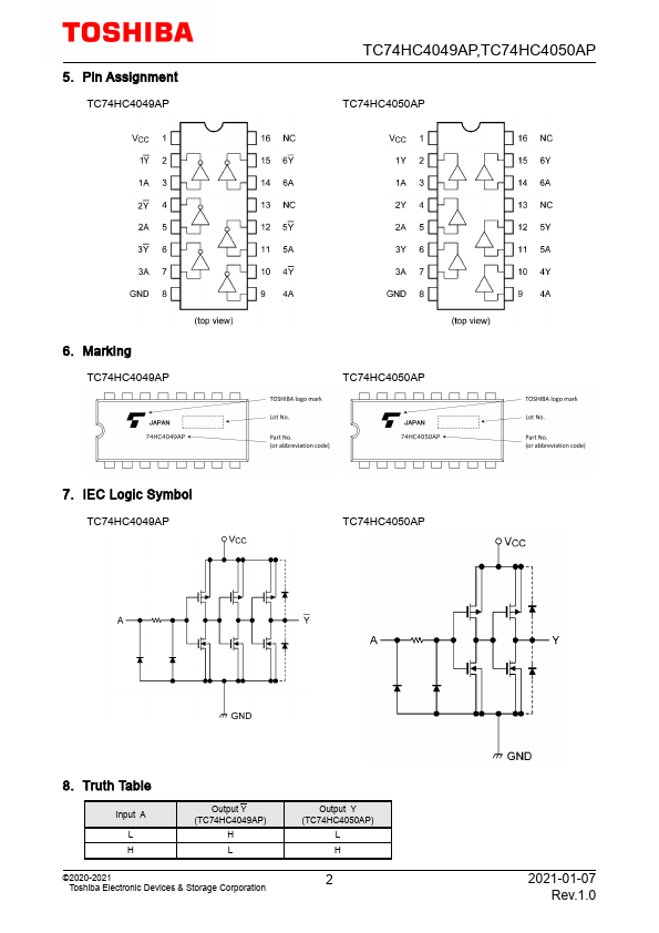
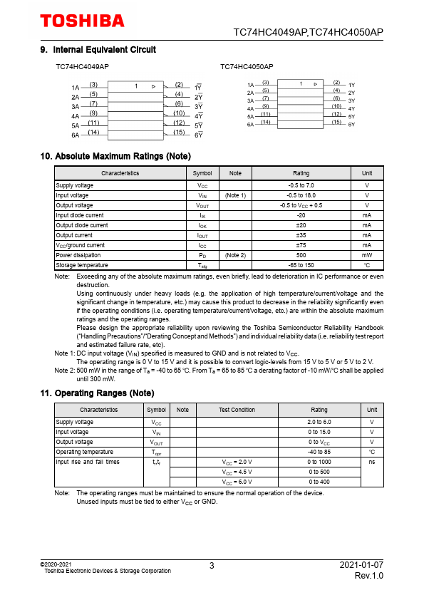
The TC74HC4049AP and TC74HC4050AP are high speed CMOS HEX BUFFERs fabricated with silicon gate C2MOS technology.
| Part number | TC74HC4049AP |
|---|---|
| Manufacturer | Toshiba |
| File Size | 210.37 KB |
| Description | HEX BUFFER/CONVERTER |
| Datasheet |
TC74HC4049AP Datasheet
|
|
|
|
Note: Below is a high-fidelity text extraction (approx. 800 characters) for TC74HC4049AP. For precise diagrams, and layout, please refer to the original PDF.
TC74HC4049AP,TC74HC4050AP CMOS Digital Integrated Circuits Silicon Monolithic TC74HC4049AP,TC74HC4050AP 1. Functional Description • Hex Buffer TC74HC4049AP: HEX BUFFER/CO...
| Part Number | Description |
|---|---|
| TC74HC4049AF | HEX BUFFER/CONVERTER |
| TC74HC4049AFT | HEX BUFFER/CONVERTER |
| TC74HC4002AF | Dual 4-Input NOR Gate |
| TC74HC4002AP | Dual 4-Input NOR Gate |
| TC74HC40102AF | Dual BCD Programmable Down Counter |
| TC74HC40102AP | Dual BCD Programmable Down Counter |
| TC74HC40103AF | 8-Bit Binary Programmable Down Counter |
| TC74HC40103AP | 8-Bit Binary Programmable Down Counter |
| TC74HC40105AF | 4-Bit x 16 Word FIFO Register |
| TC74HC40105AP | 4-Bit x 16 Word FIFO Register |