Datasheet Details
| Part number | TC74HC40105AF |
|---|---|
| Manufacturer | Toshiba |
| File Size | 322.08 KB |
| Description | 4-Bit x 16 Word FIFO Register |
| Datasheet |
 TC74HC40105AF Datasheet TC74HC40105AF Datasheet
|
|
|
Download the TC74HC40105AF datasheet PDF. This datasheet also covers the TC74HC40105AP variant, as both devices belong to the same 4-bit x 16 word fifo register family and are provided as variant models within a single manufacturer datasheet.
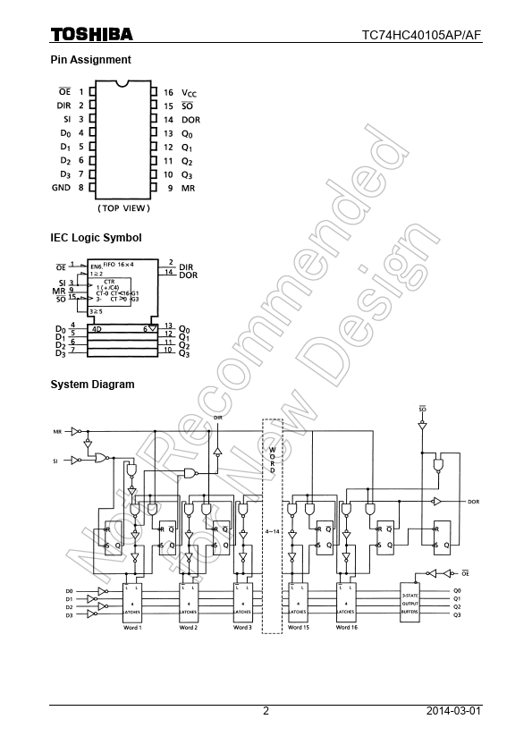
SI pin.
DIR will toggle momentarily until the data has been transferred to the second word register.
SI must be toggled before the next 4-bit word can be written.
| Part number | TC74HC40105AF |
|---|---|
| Manufacturer | Toshiba |
| File Size | 322.08 KB |
| Description | 4-Bit x 16 Word FIFO Register |
| Datasheet |
TC74HC40105AF Datasheet
|
|
|
|
Note: Below is a high-fidelity text extraction (approx. 800 characters) for TC74HC40105AF. For precise diagrams, and layout, please refer to the original PDF.
TC74HC40105AP/AF TOSHIBA CMOS Digital Integrated Circuit Silicon Monolithic TC74HC40105AP, TC74HC40105AF 4 Bit × 16 Word FIFO Register The TC74HC40105A is a high speed CM...
| Part Number | Description |
|---|---|
| TC74HC40105AP | 4-Bit x 16 Word FIFO Register |
| TC74HC40102AF | Dual BCD Programmable Down Counter |
| TC74HC40102AP | Dual BCD Programmable Down Counter |
| TC74HC40103AF | 8-Bit Binary Programmable Down Counter |
| TC74HC40103AP | 8-Bit Binary Programmable Down Counter |
| TC74HC4017AF | Decade Counter/Divider |
| TC74HC4017AP | Decade Counter/Divider |
| TC74HC4002AF | Dual 4-Input NOR Gate |
| TC74HC4002AP | Dual 4-Input NOR Gate |
| TC74HC4024AF | 7-Stage Binary Counter |