Click to expand full text
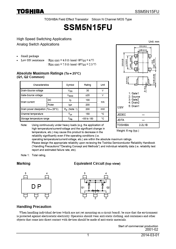
SSM5N15FU
TOSHIBA Field Effect Transistor Silicon N Channel MOS Type
SSM5N15FU
High Speed Switching Applications Analog Switch Applications
Unit: mm
• Small package • Low ON resistance : RDS (ON) = 4.0 Ω (max) (@VGS = 4 V)
: RDS (ON) = 7.0 Ω (max) (@VGS = 2.5 V)
Absolute Maximum Ratings (Ta = 25°C)
(Q1, Q2 Common)
Characteristics
Symbol
Rating
Unit
Drain-Source voltage
VDS
30
V
Gate-Source voltage
VGSS
±20
V
Drain current
DC Pulse
ID
100
mA
IDP
200
Drain power dissipation (Ta = 25°C)
PD (Note 1)
200
mW
Channel temperature
Tch
150
°C
Storage temperature range
Tstg
−55 to 150
°C
1: Gate1 2: Source 3: Gate2 4: Drain2
5: Drain1
JEDEC
―
JEITA
―
Note:
Using continuously under heavy loads (e.g.
 SSM5N15FU Datasheet