Datasheet Details
| Part number | SLGSSTVF16859V |
|---|---|
| Manufacturer | Silego |
| File Size | 336.09 KB |
| Description | DDR 13 to 26 Bit Registered Buffer |
| Datasheet |
 SLGSSTVF16859V Datasheet SLGSSTVF16859V Datasheet
|
|
|
Download the SLGSSTVF16859V datasheet PDF. This datasheet also covers the SLGSSTVF16859H variant, as both devices belong to the same ddr 13 to 26 bit registered buffer family and are provided as variant models within a single manufacturer datasheet.
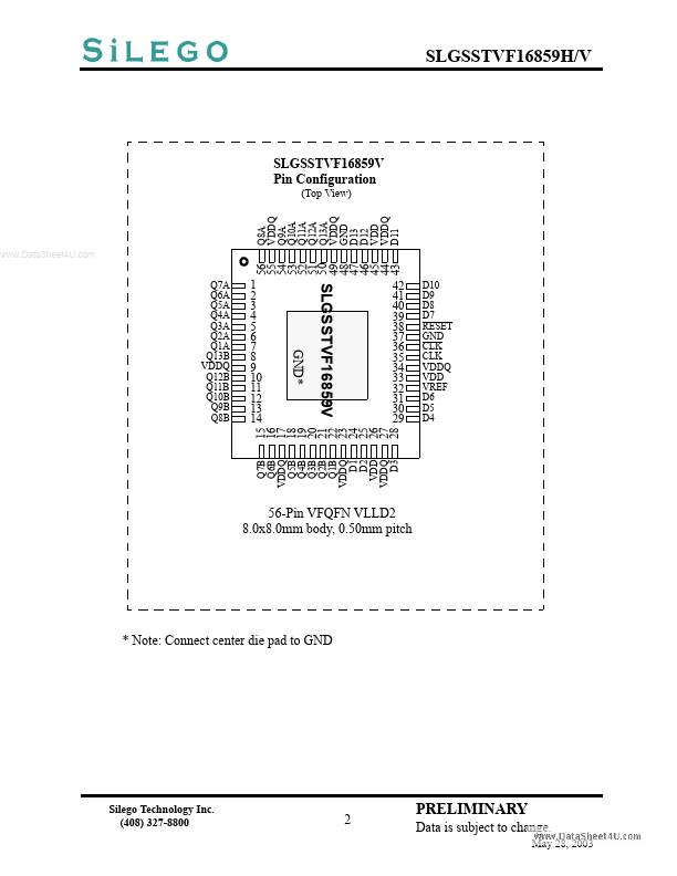
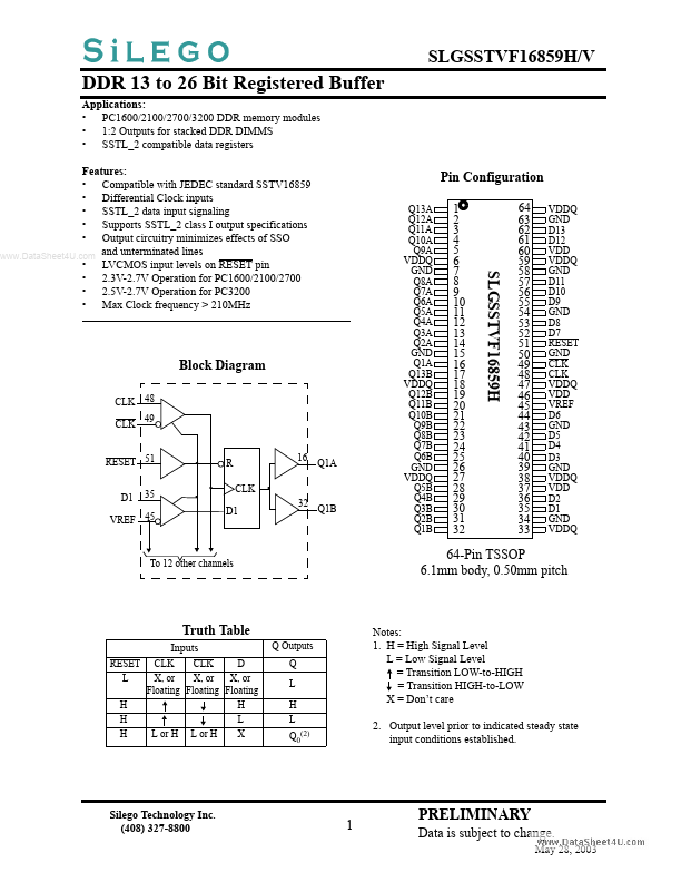
The 14-bit SLGSSTVF16859 is a registered buffer designed for 2.3V to 2.7V VDD operating range.
Inputs are SSTL_2 levels, except for the LVCMOS RESET input.
Data propagation from D to Q is controlled by the differential clock (CLK/CLK) and a control signal (RESET).
| Part number | SLGSSTVF16859V |
|---|---|
| Manufacturer | Silego |
| File Size | 336.09 KB |
| Description | DDR 13 to 26 Bit Registered Buffer |
| Datasheet |
SLGSSTVF16859V Datasheet
|
|
|
|
| Part Number | Description | Manufacturer |
|---|---|---|
| SLGSSTU32864E | DDR2 Configurable Registered Buffer | ETC |
| SLG | CONDUCTIVE POLYMER ALUMINUM SOLID ELECTROLYTIC CAPACITORS | Rubycon |
| SLG2016 | Alphanumeric Intelligent Display DEVICES | Infineon Technologies |
| SLG46108 | Ultra-small Programmable Mixed-signal Matrix | Renesas |
| SLG46110 | Programmable Mixed-Signal Matrix | Renesas |
| Part Number | Description |
|---|---|
| SLGSSTVF16859H | DDR 13 to 26 Bit Registered Buffer |
| SLG3NB3331 | 32.768 kHz and MHz GreenCLK |
| SLG3SY3952 | 1:3 Clock Buffer |
| SLG46116 | GreenPAK Programmable Mixed-signal Matrix |
| SLG46117 | GreenPAK Programmable Mixed-signal Matrix |
The following content is an automatically extracted verbatim text from the original manufacturer datasheet and is provided for reference purposes only.