Datasheet Details
| Part number | SLGSSTU32864E |
|---|---|
| Manufacturer | Unknown Manufacturer |
| File Size | 206.94 KB |
| Description | DDR2 Configurable Registered Buffer |
| Datasheet |
 SLGSSTU32864E Datasheet SLGSSTU32864E Datasheet
|
|
|
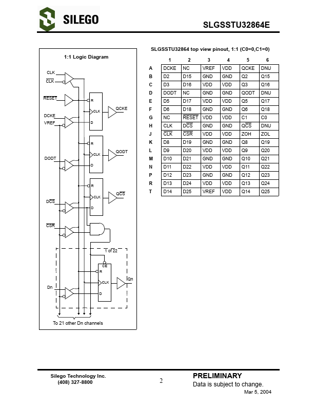
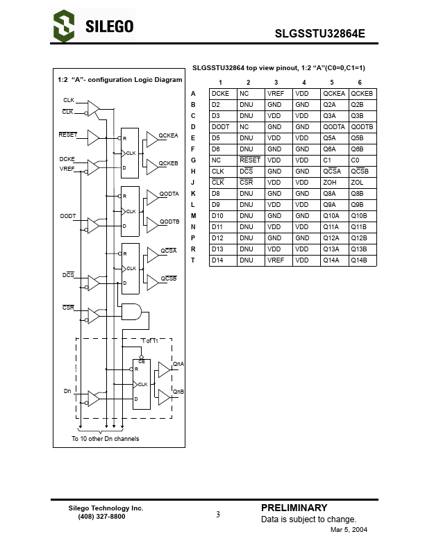
The SLGSSTU32864 is a configurable registered buffer designed for 1.7V to 1.9V VDD operating range.
When C1 input pin is low, the SLGSSTU32864 is 1:1 25-bit configuration.
When C1 input pin is high, the SLGSSTU32864 is 1:2 14-bit configuration.
| Part number | SLGSSTU32864E |
|---|---|
| Manufacturer | Unknown Manufacturer |
| File Size | 206.94 KB |
| Description | DDR2 Configurable Registered Buffer |
| Datasheet |
SLGSSTU32864E Datasheet
|
|
|
|
| Part Number | Description | Manufacturer |
|---|---|---|
| SLGSSTVF16859H | DDR 13 to 26 Bit Registered Buffer | Silego |
| SLGSSTVF16859V | DDR 13 to 26 Bit Registered Buffer | Silego |
| SLG | CONDUCTIVE POLYMER ALUMINUM SOLID ELECTROLYTIC CAPACITORS | Rubycon |
| SLG2016 | Alphanumeric Intelligent Display DEVICES | Infineon Technologies |
| SLG3NB3331 | 32.768 kHz and MHz GreenCLK | Silego |
| Part Number | Description |
|---|
The following content is an automatically extracted verbatim text from the original manufacturer datasheet and is provided for reference purposes only.