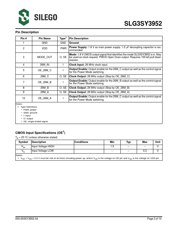
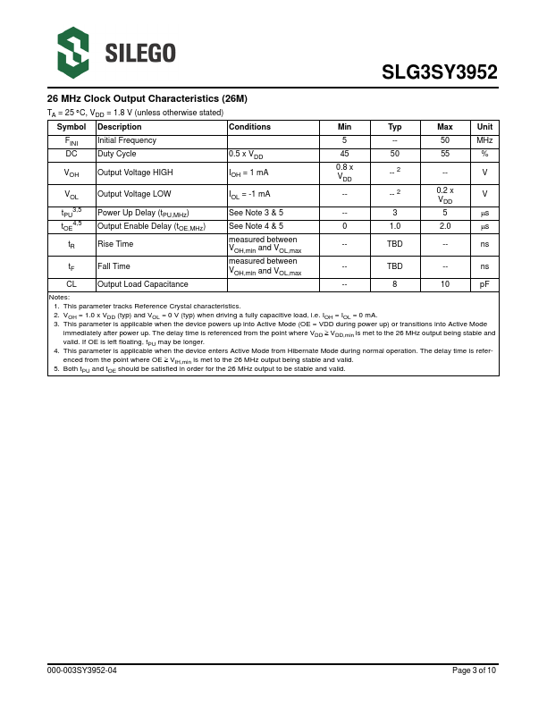
Click to expand full text
SLG3SY3952
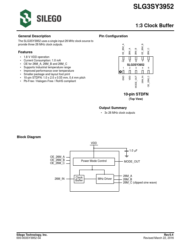
1:3 Clock Buffer
OE_26M_A 26M_A 26M_B OE_26M_B 26M_C
General Description
The SLG3SY3952 uses a single input 26 MHz clock source to provide three 26 MHz clock outputs.
Pin Configuration
Features
• 1.8 V VDD operation • Current Consumption: 1.0 mA • OE for 26M_A, 26M_B and 26M_C • Supports Industrial temperature range • Improved performance over temperature • Smaller package and layout foot print • 10-pin STDFN: 1.0 x 2.0 x 0.55 mm, 0.4 mm pitch • Pb-Free / Halogen-Free / RoHS compliant
10 9 8 7
SLG3SY3952
1 23 4
6 5
GND VDD MODE_OUT 26M_IN OE_26M_C
10-pin STDFN
(Top View)
Output Summary
• 3x 26 MHz clock outputs
Block Diagram
OE_26M_A OE_26M_B OE_26M_C
VDD Power Mode Control
26M_IN
Clock Buffer
MHz Driver
1.
 SLG3SY3952 Datasheet