Datasheet Details
| Part number | K4T51083QC |
|---|---|
| Manufacturer | Samsung Semiconductor |
| File Size | 630.58 KB |
| Description | 512Mb C-die DDR2 SDRAM |
| Datasheet |
 K4T51083QC Datasheet K4T51083QC Datasheet
|
|
|
3.
4.
Rev.
| Part number | K4T51083QC |
|---|---|
| Manufacturer | Samsung Semiconductor |
| File Size | 630.58 KB |
| Description | 512Mb C-die DDR2 SDRAM |
| Datasheet |
K4T51083QC Datasheet
|
|
|
|
Note: Below is a high-fidelity text extraction (approx. 800 characters) for K4T51083QC. For precise diagrams, and layout, please refer to the original PDF.
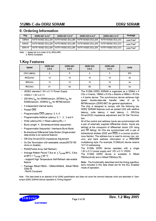
512Mb C-die DDR2 SDRAM DDR2 SDRAM 512Mb C-die DDR2 SDRAM Specification Version 1.2 May 2005 Page 1 of 29 Rev. 1.2 May 2005 512Mb C-die DDR2 SDRAM Contents DDR2 SDRAM 0. O...
| Brand Logo | Part Number | Description | Manufacturer |
|---|---|---|---|
| K4T51083QB-GCD5 | 512Mb B-die DDR2 SDRAM | Samsung semiconductor | |
| K4T51083QB-ZCD5 | 512Mb B-die DDR2 SDRAM | Samsung semiconductor | |
| K4T51083QE | 512Mb E-die DDR2 SDRAM Specification | Samsung semiconductor |
| Part Number | Description |
|---|---|
| K4T51083QG | 512Mb G-die DDR2 SDRAM |
| K4T51083QI | 512Mb I-die DDR2 SDRAM |
| K4T51083QJ | 512Mb J-die DDR2 SDRAM |
| K4T51083QN | 512Mb N-die DDR2 SDRAM |
| K4T51083QQ | 512Mb Q-die DDR2 SDRAM |
| K4T51043Q | 512Mb B-die DDR2 SDRAM |
| K4T51043QG | 512Mb G-die DDR2 SDRAM |
| K4T51043QI | 512Mb I-die DDR2 SDRAM |
| K4T51043QJ | 512Mb J-die DDR2 SDRAM |
| K4T51163QB | 512Mb B-die DDR2 SDRAM |