Datasheet Details
| Part number | K4H561638D-TCB3 |
|---|---|
| Manufacturer | Samsung Semiconductor |
| File Size | 205.14 KB |
| Description | 256Mb D-die DDR Sdram |
| Datasheet |
 K4H561638D-TCB3 Datasheet K4H561638D-TCB3 Datasheet
|
|
|
Download the K4H561638D-TCB3 datasheet PDF. This datasheet also covers the K4H560838D-TCB3 variant, as both devices belong to the same 256mb d-die ddr sdram family and are provided as variant models within a single manufacturer datasheet.
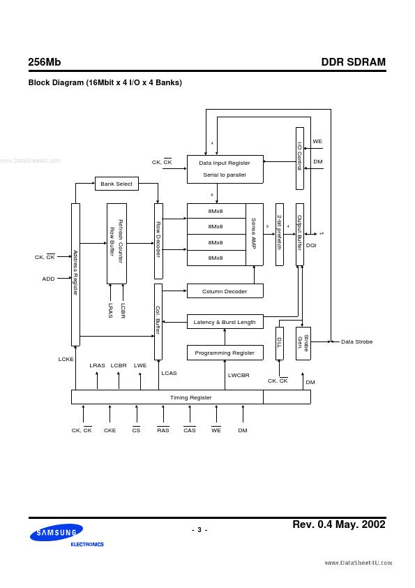
Clock : CK and CK are differential clock inputs.
All address and control input signals are sampled on the positive edge of CK and negative edge of CK.
Output (read) data is referenced to both edges of CK.
| Part number | K4H561638D-TCB3 |
|---|---|
| Manufacturer | Samsung Semiconductor |
| File Size | 205.14 KB |
| Description | 256Mb D-die DDR Sdram |
| Datasheet |
K4H561638D-TCB3 Datasheet
|
|
|
|
Note: Below is a high-fidelity text extraction (approx. 800 characters) for K4H561638D-TCB3. For precise diagrams, and layout, please refer to the original PDF.
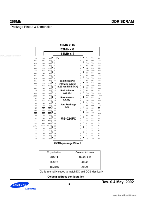
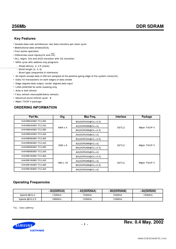
256Mb Key Features • Double-data-rate architecture; two data transfers per clock cycle • Bidirectional data strobe(DQS) • Four banks operation • Differential clock inputs...
| Part Number | Description |
|---|---|
| K4H561638F | 256Mb F-die DDR SDRAM Specification |
| K4H561638F-TCC4 | 256Mb F-die DDR400 SDRAM Specification |
| K4H561638F-TCCC | 256Mb F-die DDR400 SDRAM Specification |
| K4H561638F-UCC4 | 256Mb F-die DDR400 SDRAM |
| K4H561638F-UCCC | 256Mb F-die DDR400 SDRAM |
| K4H561638H | (K4H560438H - K4H561638H) 256Mb H-die DDR SDRAM Specification |
| K4H561638J | 256Mb J-die DDR SDRAM Specification |
| K4H560438D-TCB3 | 256Mb D-die DDR Sdram |
| K4H560438H | (K4H560438H - K4H561638H) 256Mb H-die DDR SDRAM Specification |
| K4H560438J | 256Mb J-die DDR SDRAM Specification |