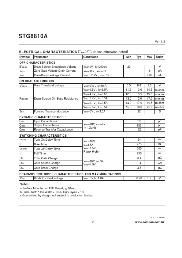
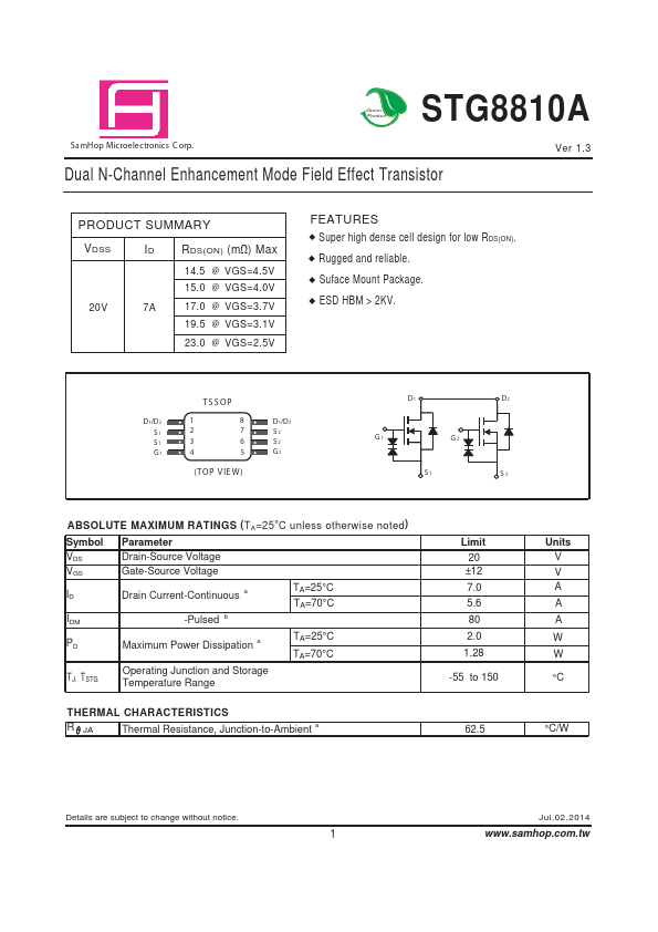
STG8810A - Dual N-Channel Enhancement Mode Field Effect Transistor
Features
Super high dense cell design for low R DS(ON). Rugged and reliable. Suface Mount Package. ESD HBM > 2KV. T S S OP
D 1/D 2 S1 S1 G1 1 2 3 4 8 7 6 5 D 1/D 2 S2 S2 G2
D1
D2
G1
G2
(T OP V IE W)
S1
S2.
STG8810- Dual N-Channel Enhancement Mode Field Effect Transistor
STG8820- Dual N-Channel Enhancement Mode Field Effect Transistor
STG8203- Dual N-Channel Enhancement Mode Field Effect Transistor
STG8205- Dual N-Channel Enhancement Mode Field Effect Transistor
STG8206- Dual N-Channel Enhancement Mode Field Effect Transistor
STG8207- Dual N-Channel Enhancement Mode Field Effect Transistor
STG8209- Dual N-Channel Enhancement Mode Field Effect Transistor
STG8210- Dual N-Channel Enhancement Mode Field Effect Transistor
Full PDF Text Transcription
Click to expand full text
Green Product
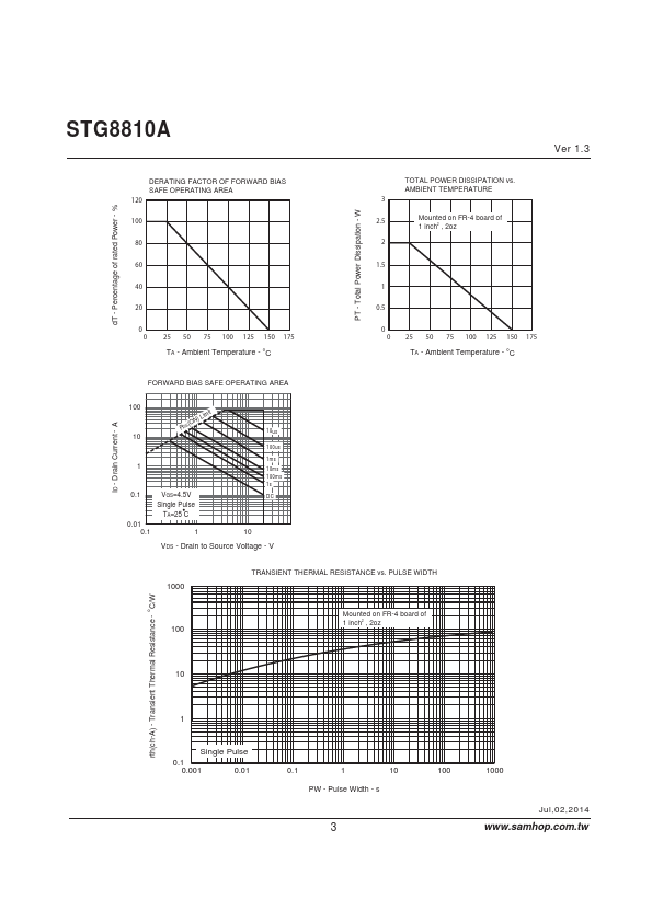
STG8810A
Ver 1.3
S a mHop Microelectronics C orp.
Dual N-Channel Enhancement Mode Field Effect Transistor
PRODUCT SUMMARY
V DSS ID R DS(ON) (m Ω) Max
14.5 @ VGS=4.5V 15.0 @ VGS=4.0V 20V 7A 17.0 @ VGS=3.7V 19.5 @ VGS=3.1V 23.0 @ VGS=2.5V
FEATURES Super high dense cell design for low R DS(ON). Rugged and reliable. Suface Mount Package. ESD HBM > 2KV.
T S S OP
D 1/D 2 S1 S1 G1 1 2 3 4 8 7 6 5 D 1/D 2 S2 S2 G2
D1
D2
G1
G2
(T OP V IE W)
S1
S2
ABSOLUTE MAXIMUM RATINGS ( T A=25 °C unless otherwise noted ) Symbol VDS VGS ID IDM PD TJ, TSTG Parameter Drain-Source Voltage Gate-Source Voltage Drain Current-Continuous -Pulsed
b a
Limit 20 ±12 TA=25°C TA=70°C TA=25°C TA=70°C 7.0 5.6 80
a
Units V V A A A W W °C
Maximum Power Dissipation
2.0 1.
 STG8810A Datasheet