Click to expand full text
www.DataSheet4U.com
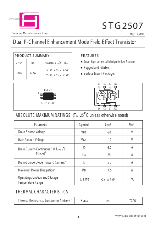
S T G 2507
S amHop Microelectronics C orp. May,10 2005
Dual P -C hannel E nhancement Mode Field E ffect Transistor
P R ODUC T S UMMAR Y
V DS S
-20V
F E AT UR E S
( mW ) Max
ID
6.2A
R DS (ON)
S uper high dense cell design for low R DS (ON ).
17 @ V G S = -4.5V 25 @ V G S = -2.5V
R ugged and reliable. S urface Mount P ackage.
D2
8
S2
7
S2
6
G2
5
T S S OP
1
(T OP V IE W)
1 2 3 4
D1
S1
S1
G1
ABS OLUTE MAXIMUM R ATINGS (T A=25 C unless otherwise noted)
P arameter Drain-S ource Voltage Gate-S ource Voltage Drain C urrent-C ontinuous a @ T J =25 C b -P ulsed Drain-S ource Diode Forward C urrent a Maximum P ower Dissipation a Operating Junction and S torage Temperature R ange S ymbol V DS V GS ID IDM IS PD T J , T S TG Limit -20 12 -6.2 -25 -1.7 1.
 STG2507 Datasheet