Click to expand full text
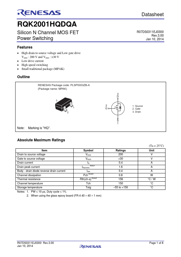
RQK2001HQDQA
Silicon N Channel MOS FET Power Switching
Features
• High drain to source voltage and Low gate drive VDSS : 200 V and VGSS : ±30 V
• Low drive current • High speed switching • Small traditional package (MPAK)
Outline
RENESAS Package code: PLSP0003ZB-A (Package name: MPAK)
3
1 2
Note: Marking is "HQ".
Preliminary Datasheet
R07DS0311EJ0300 Rev.3.00
Jan 10, 2014
3 D
2 G
S 1
1. Source 2. Gate 3. Drain
Absolute Maximum Ratings
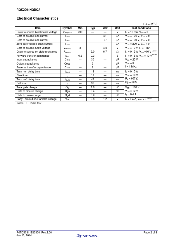
Item
Symbol
Drain to source voltage Gate to source voltage Drain current Drain peak current Body - drain diode reverse drain current Channel dissipation Thermal resistance
VDSS
VGSS
ID ID(pulse) Note1
IDR Pch Note2 Rth(ch-a) Note2
Channel temperature
Tch
Storage temperature
Tstg
Notes: 1. PW ≤ 10 μs, Duty cycle ≤ 1%
2.
 RQK2001HQDQA Datasheet