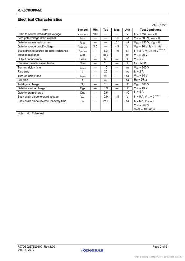
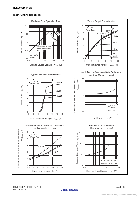
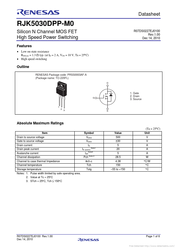
Datasheet4U Logo Datasheet4U.com

RJK5030DPP-M0 - High Speed Power Switching

Description

of circuits, software and other related information in this document are provided only to illustrate the operation of semiconductor products and application examples.

You are fully responsible for the incorporation of these circuits, software, and information in the design of your equipment.

Features

  • Low on-state resistance RDS(on) = 1.3  typ. (at ID = 2 A, VGS = 10 V, Ta = 25C).
  • High speed switching R07DS0227EJ0100 Rev.1.00 Dec 14, 2010 Outline.

📥 Download Datasheet

Datasheet preview – RJK5030DPP-M0

Datasheet Details

Part number RJK5030DPP-M0
Manufacturer Renesas
File Size 99.02 KB
Description High Speed Power Switching
Datasheet download datasheet RJK5030DPP-M0 Datasheet
Additional preview pages of the RJK5030DPP-M0 datasheet.
Other Datasheets by Renesas

Full PDF Text Transcription

Click to expand full text
Preliminary Datasheet RJK5030DPP-M0 Silicon N Channel MOS FET High Speed Power Switching Features  Low on-state resistance RDS(on) = 1.3  typ. (at ID = 2 A, VGS = 10 V, Ta = 25C)  High speed switching R07DS0227EJ0100 Rev.1.00 Dec 14, 2010 Outline RENESAS Package code: PRSS0003AF-A (Package name: TO-220FL) D G 1. Gate 2. Drain 3. Source 1 2 3 S Absolute Maximum Ratings (Ta = 25C) Item Drain to source voltage Gate to source voltage Drain current Drain peak current Avalanche current Channel dissipation Channel to case thermal Impedance Channel temperature Storage temperature Notes: 1. Pulse width limited by safe operating area. 2. Value at Tc = 25C 3. STch = 25C, Tch  150C Symbol VDSS VGSS ID ID (pulse) Note3 IAP Pch Note 2 ch-c Tch Tstg Note1 Value 500 30 5 20 5 28.5 4.
Published: |