Click to expand full text
Preliminary Datasheet
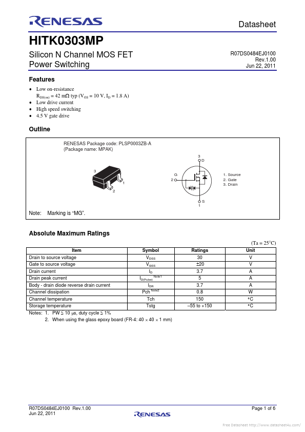
HITK0303MP
Silicon N Channel MOS FET Power Switching
Features
Low on-resistance RDS(on) = 42 m typ (VGS = 10 V, ID = 1.8 A) Low drive current High speed switching 4.5 V gate drive R07DS0484EJ0100 Rev.1.00 Jun 22, 2011
Outline
RENESAS Package code: PLSP0003ZB-A (Package name: MPAK)
3 D 3 1 2 S 1 2
G
1. Source 2. Gate 3. Drain
Note:
Marking is “MG”.
Absolute Maximum Ratings
(Ta = 25°C)
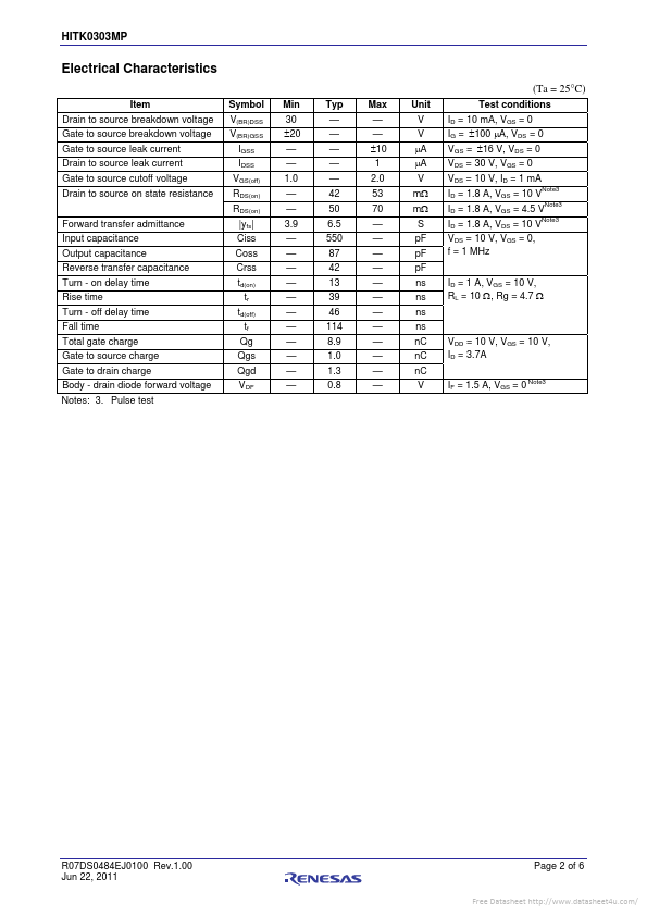
Item Drain to source voltage Gate to source voltage Drain current Drain peak current Body - drain diode reverse drain current Channel dissipation Channel temperature Storage temperature Symbol VDSS VGSS ID ID(Pulse) Note1 IDR Pch Note2 Tch Tstg Ratings 30 20 3.7 5 3.7 0.8 150 –55 to +150 Unit V V A A A W C C
Notes: 1. PW 10 s, duty cycle 1% 2.
 HITK0303MP Datasheet