Datasheet Details
| Part number | HD74CDCV857A |
|---|---|
| Manufacturer | Renesas |
| File Size | 235.33 KB |
| Description | 2.5-V Phase-lock Loop Clock Driver |
| Datasheet |
 HD74CDCV857A Datasheet HD74CDCV857A Datasheet
|
|
|
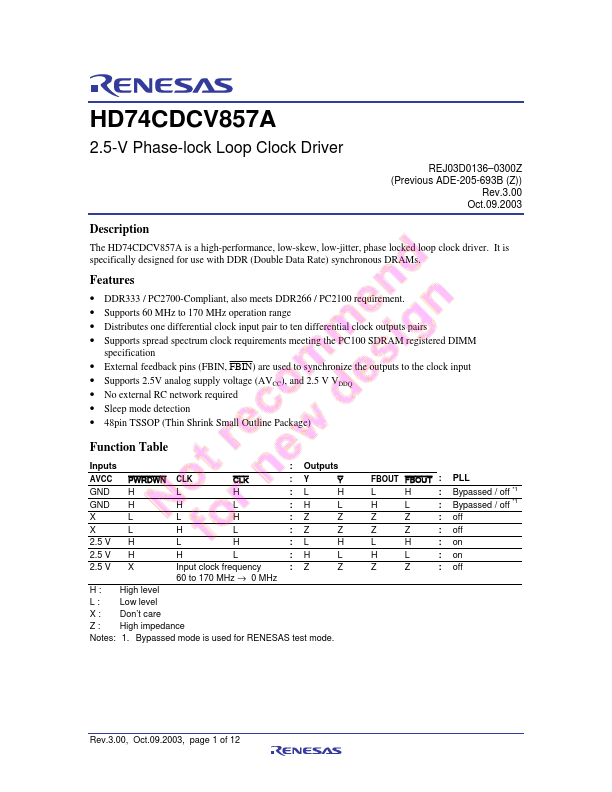
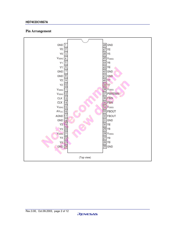
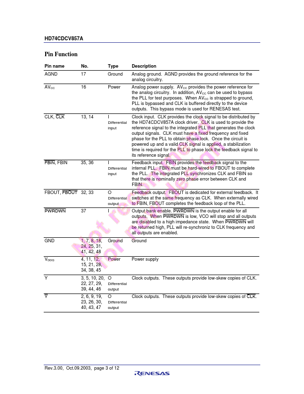
The HD74CDCV857A is a high-performance, low-skew, low-jitter, phase locked loop clock driver.
It is specifically designed for use with DDR (Double Data Rate) synchronous DRAMs.
| Part number | HD74CDCV857A |
|---|---|
| Manufacturer | Renesas |
| File Size | 235.33 KB |
| Description | 2.5-V Phase-lock Loop Clock Driver |
| Datasheet |
HD74CDCV857A Datasheet
|
|
|
|