Click to expand full text
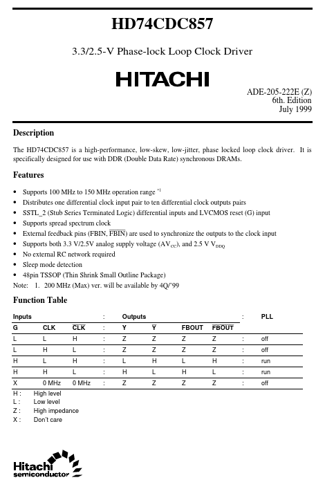
HD74CDC857
3.3/2.5-V Phase-lock Loop Clock Driver
ADE-205-222E (Z) 6th. Edition July 1999 Description
The HD74CDC857 is a high-performance, low-skew, low-jitter, phase locked loop clock driver. It is specifically designed for use with DDR (Double Data Rate) synchronous DRAMs.
Features
• Supports 100 MHz to 150 MHz operation range *1 • Distributes one differential clock input pair to ten differential clock outputs pairs • SSTL_2 (Stub Series Terminated Logic) differential inputs and LVCMOS reset (G) input • Supports spread spectrum clock • External feedback pins (FBIN, FBIN) are used to synchronize the outputs to the clock input • Supports both 3.3 V/2.5V analog supply voltage (AV CC), and 2.
 HD74CDC857 Datasheet