Click to expand full text
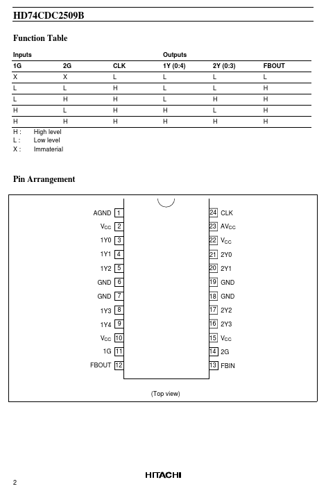
HD74CDC2509B
3.3-V Phase-lock Loop Clock Driver
ADE-205-218F (Z) 7th. Edition October 1999 Description
The HD74CDC2509B is a high-performance, low-skew, low-jitter, phase-lock loop clock driver. It uses a phase-lock loop (PLL) to precisely align, in both frequency and phase, the feedback (FBOUT) output to the clock (CLK) input signal. It is specifically designed for use with synchronous DRAMs. The HD74CDC2509B operates at 3.3 V V CC and is designed to drive up to five clock loads per output. One bank of five outputs and one bank of four outputs provide nine low-skew, low-jitter copies of the input clock. Output signal duty cycles are adjusted to 50 percent independent of the duty cycle at the input clock.
 HD74CDC2509B Datasheet