Click to expand full text
HD74ALVC2G245
Dual Bus Transceivers with 3-state Output
REJ03D0176–0400Z (Previous ADE-205-641C (Z))
Rev.4.00 Dec.18.2003
Description
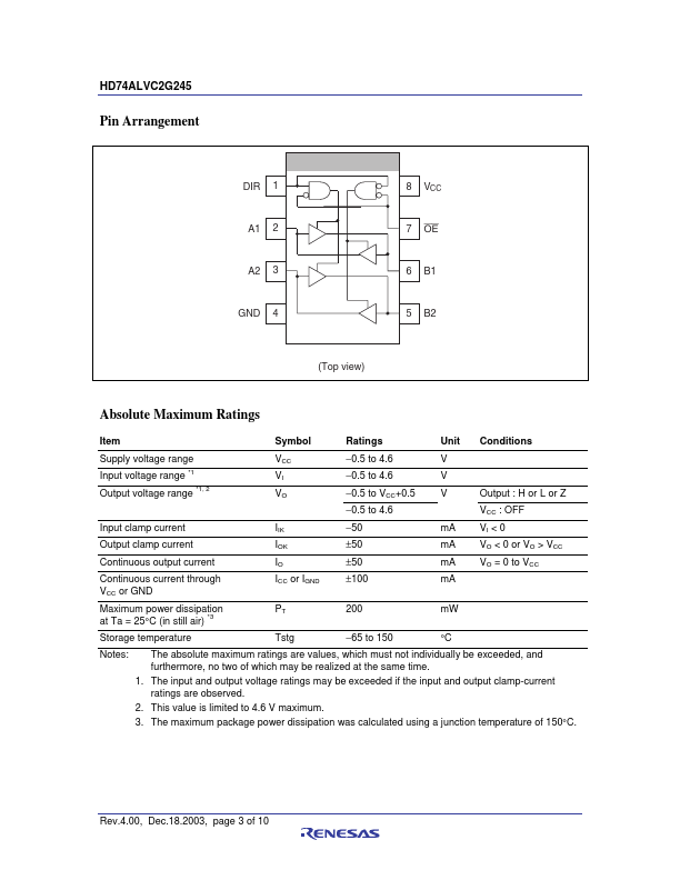
The HD74ALVC2G245 has two buffers with three state output in an 8 pin package. When DIR is high, data is transferred from the A inputs to the B outputs, and when DIR is low, data is transferred from the B inputs to the A outputs. The A and B buses are separated by making the enable input (OE) high level. Low voltage and high-speed operation is suitable for the battery powered products (e.g., notebook computers), and the low power consumption extends the battery life.
Features
• The basic gate function is lined up as Renesas uni logic series.
• Supplied on emboss taping for high-speed automatic mounting.
• Supply voltage range : 1.2 to 3.
 HD74ALVC2G245 Datasheet