Click to expand full text
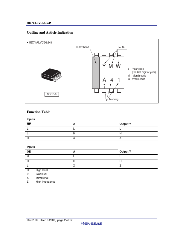
HD74ALVC2G241
Dual Bus Buffer Noninverted with 3-state Output
REJ03D0175–0200Z (Previous ADE-205-573A (Z))
Rev.2.00 Dec.18.2003
Description
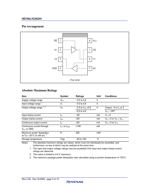
The HD74ALVC2G241 has dual bus buffer noninverted with 3-state output in an 8 pin package. Two noninverters are included in one circuit. Each circuit can be independently controlled by the enable signal OE or OE, which enables outputs when receiving a low or high-level signal, respectively. To ensure the high impedance state during power up or power down, OE should be connected to VCC through a pull-up resistor; the minimum value of the resistor is determined by the current sinking capability of the driver. Low voltage and high-speed operation is suitable for the battery powered products (e.g.
 HD74ALVC2G241 Datasheet