The following content is an automatically extracted verbatim text
from the original manufacturer datasheet and is provided for reference purposes only.
View original datasheet text
www.DataSheet4U.com
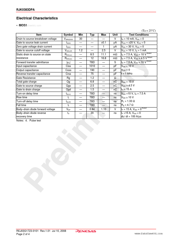
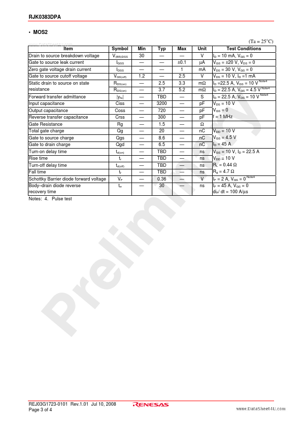
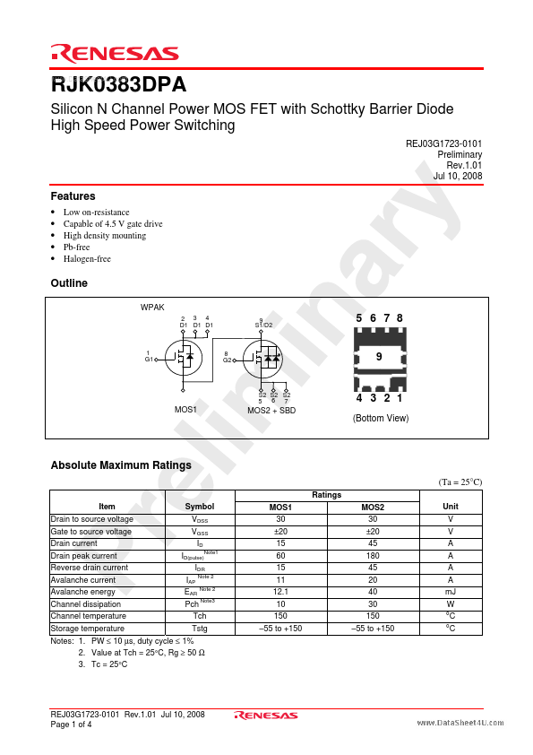
RJK0383DPA
Silicon N Channel Power MOS FET with Schottky Barrier Diode High Speed Power Switching
REJ03G1723-0101 Preliminary Rev.1.01 Jul 10, 2008
Features
• • • • • Low on-resistance Capable of 4.5 V gate drive High density mounting Pb-free Halogen-free
Outline
WPAK
2 3 4 D1 D1 D1
9 S1/D2
5 6 7 8
1 G1
8 G2
9
S2 S2 S2 6 7 5
4 3 2 1
(Bottom View)
MOS1
MOS2 + SBD
Absolute Maximum Ratings
(Ta = 25°C)
Ratings Item Drain to source voltage Gate to source voltage Drain current Drain peak current Reverse drain current Avalanche current Avalanche energy Channel dissipation Channel temperature Storage temperature Symbol VDSS VGSS ID ID(pulse)Note1 IDR IAP Note 2 EAR Note 2 Pch Note3 Tch Tstg MOS1 30 ±20 15 60 15 11 12.
 RJK0383DPA Datasheet