Click to expand full text
www.DataSheet4U.com
HAT2281C
Silicon N Channel MOS FET Power Switching
REJ03G1328-0200 Rev.2.00 Jan 26, 2006
Features
• Low on-resistance RDS(on) = 109 mΩ typ.(at VGS = 4.5 V) • Low drive current • High density mounting • 2.5 V gate drive device
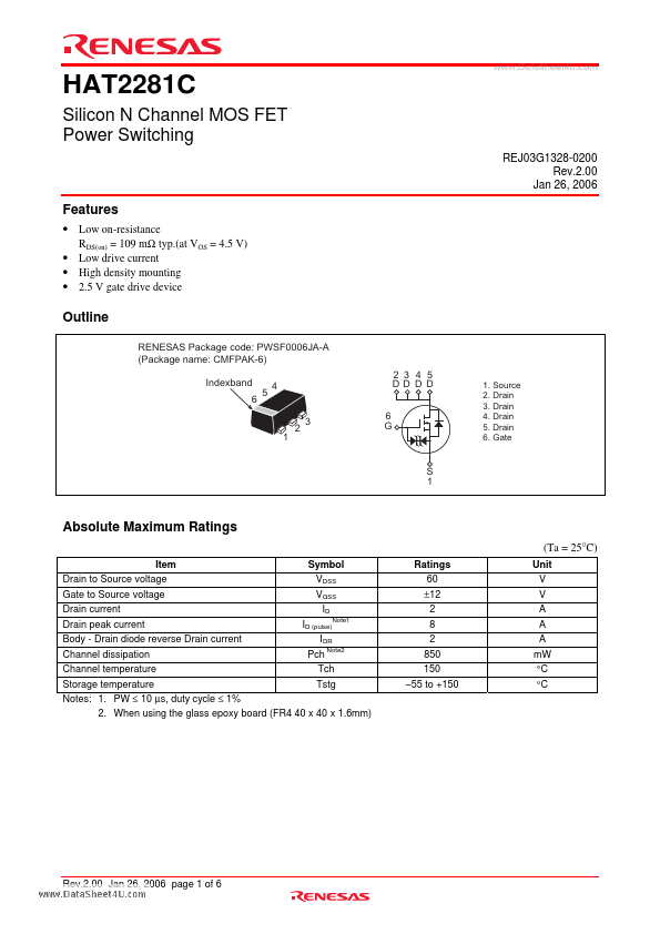
Outline
RENESAS Package code: PWSF0006JA-A (Package name: CMFPAK-6) Indexband 6 5 4 6 G 2 3 4 5 DD D D
1. Source 2. Drain 3. Drain 4. Drain 5. Drain 6. Gate
1
2
3
S 1
Absolute Maximum Ratings
(Ta = 25°C)
Item Symbol Drain to Source voltage VDSS Gate to Source voltage VGSS Drain current ID Note1 Drain peak current ID (pulse) Body - Drain diode reverse Drain current IDR Channel dissipation Pch Note2 Channel temperature Tch Storage temperature Tstg Notes: 1. PW ≤ 10 µs, duty cycle ≤ 1% 2. When using the glass epoxy board (FR4 40 x 40 x 1.
 HAT2281C Datasheet