PPMT30V3
Description
The enhancement mode MOS is extremely high density cell and low on-resistance.
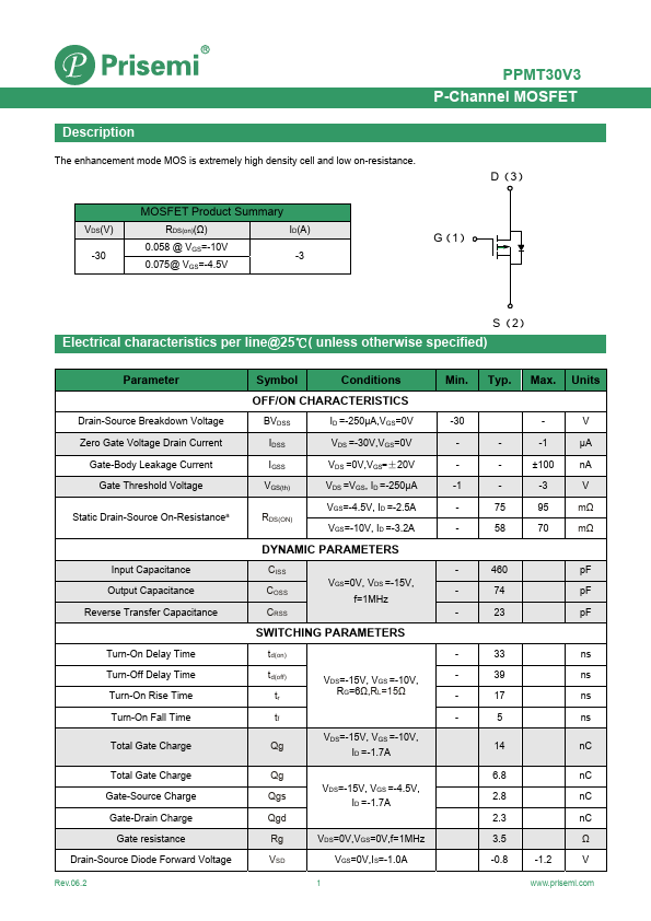
D(3)
VDS(V) -30
MOSFET Product Summary
RDS(on)(Ω)
ID(A)
0.058 @ VGS=-10V -3
0.075@ VGS=-4.5V
G(1)
S(2)
Electrical characteristics per line@25℃( unless otherwise specified)
Parameter
Drain-Source Breakdown Voltage Zero Gate Voltage Drain Current
Gate-Body Leakage Current Gate Threshold Voltage
Static Drain-Source On-Resistancea
Input Capacitance Output Capacitance Reverse Transfer Capacitance
Turn-On Delay Time Turn-Off Delay Time Turn-On Rise Time Turn-On Fall Time Total Gate Charge Total Gate Charge Gate-Source Charge Gate-Drain Charge
Gate resistance Drain-Source Diode Forward Voltage
Rev.06.2
Symbol
Conditions
OFF/ON CHARACTERISTICS
BVDSS
ID =-250μA,VGS=0V
IDSS
VDS =-30V,VGS=0V
IGSS
VDS =0V,VGS=±20V
VGS(th)
VDS =VGS, ID =-250μA
RDS(ON)
VGS=-4.5V, ID =-2.5A VGS=-10V, ID =-3.2A
DYNAMIC PARAMETERS
CISS COSS CRSS
VGS=0V, VDS =-15V, f=1MHz
SWITCHING PARAMETERS td(on)...