PNM3FD20V2
Description
The MOSFET provide the best bination of fast switching , low on-resistance and cost-effectiveness.
MOSFET Product Summary
VDS(V) 20
RDS(on)(mΩ) 62 @ VGS = 4.5V 70 @ VGS = 2.5V
ID(A) 2
Feature
- High Power and current handing capability
- Lead free product is acquired
- Surface Mount Package
Applications
- PWM applications
- Load switch
- Power management
Absolute maximum rating@25℃
Rating Drain-source Voltage Gate-source Voltage Drain Current Pulsed Drain Current Total Power Dissipation Channel to ambient Junction and Storage Temperature Range
PNM3FD20V2 N-Channel MOSFET
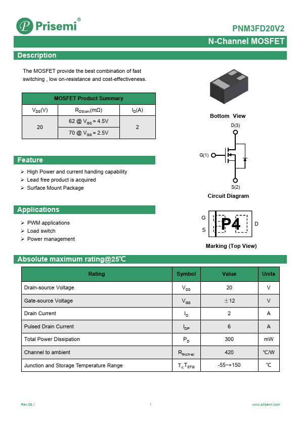
Bottom View
D(3)
G(1)
S(2)
Circuit Diagram
P4 G D S
Marking (Top View)
Symbol VDS VGS ID IDP PD
Rth(ch-a) TJ,TSTG
Value 20
±12 2 6
300 420 -55~+150
Units V V A A m W ℃/W
℃
Rev.06.1
.prisemi.
N-Channel MOSFET
Electrical characteristics per line@25℃ (unless otherwise specified)
Parameter Off Characteristics Drain-Source Breakdown Voltage Zero Gate Voltage Drain Current Gate-Body...