Click to expand full text
Preliminary
PLL103-05
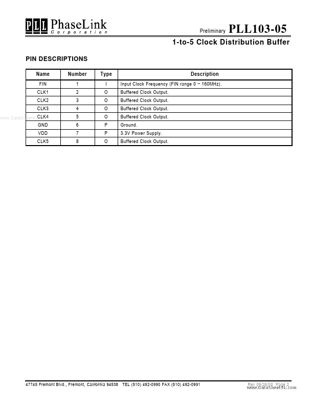
1-to-5 Clock Distribution Buffer
FEATURES
• • • • • • • 5 outputs identical to FIN. Low skew (< 250 ps between outputs). Input / Output frequency range 0 – 160 MHz 25mA drive capability at TTL levels. 70mA drive capability at CMOS levels. 3.3V operation. Available in 8-Pin 150mil SOIC.
PIN CONFIGURATION
FIN CLK1 CLK2 CLK3 1 8 CLK5 VDD GND CLK4
PLL103-05
2 3 4
7 6 5
www.DataSheet4U.com
FIN = 0 ~ 160 Mhz
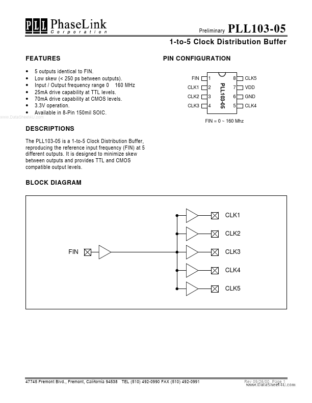
DESCRIPTIONS
The PLL103-05 is a 1-to-5 Clock Distribution Buffer, reproducing the reference input frequency (FIN) at 5 different outputs. It is designed to minimize skew between outputs and provides TTL and CMOS compatible output levels.
BLOCK DIAGRAM
CLK1 CLK2 FIN CLK3 CLK4 CLK5
47745 Fremont Blvd.
 PLL103-05 Datasheet